Topic outline
Resistor Circuits
Resistor circuits
Objective
The objective of this activity is to brush up on your existing knowledge about Kirchhoff’s laws and expand on that knowledge by showing how they can be applied in resistor circuits. A secondary outcome will be a preliminary understanding of the Red Pitaya STEMlab hardware and software - test & measurements applications.
Background
To begin this lesson, we will introduce you to a fundamental equation that is necessary for anyone interested in electronics.
\( U=R \cdot I \)
This equation serves as the foundation of resistor circuits, which includes any circuit that does not have active elements and remains unchanged for an extended period. Another equation that is useful in such circuits is the one that describes power dissipation on any resistor.
\( P=U \cdot I \)
Even though you can always determine voltage drop across, and current flowing through any resistor, it often comes handy to remember two more equations, in which voltage drop or current is substituted for its function of the other two values.
\( P=I^2 \cdot R = U^2/R \)
With this out of the way, we can move on to…
Kirchhoff’s laws
In order to solve a circuit that consists of multiple components, it is important to understand Kirchhoff's laws, which include Kirchhoff's current law (KCL) and Kirchhoff's voltage law (KVL).
“KCL states that the algebraic sum of currents in a network of conductors meeting at a point is zero. Simply put, any current entering a node must also exit the same node. “
If the first law talks about current, logic would suggest that the second law will be about voltage (KVL).
“KVL states that the directed sum of the potential differences (voltages) around any closed loop is zero.”
If these concepts are still unclear, don't worry. We will clarify them through examples later on. Before that, we will explore some equations and facts that can simplify the process of solving resistor circuits.
Some equations and facts
If there is only one voltage source in a circuit, it can be simplified using two equations for equivalent substitute resistors. This can help to easily calculate the voltage drop or current and make complex circuits easier to analyze.
\( R_{S_{series}} = R_1 + R_2 \)
\( \frac{R_{S_{parallel}}}{1} = \frac{1}{R_1} + \frac{1}{R_2} \)
When you have a circuit with only one voltage or current source and one substitute resistor, you can simplify the circuit and then work backwards to calculate the branch voltages and currents. It's important to understand what happens to currents and voltages when you branch out. If the substitute resistor is split into parallel resistors, the voltage drop across them remains the same. In contrast, when the substitute resistor is split into series resistors, the voltage is divided among them proportionally to their resistance. This is due to the behavior of current, which remains unchanged when a substitute resistor is split into multiple series resistors. While this may sound complicated, knowing these principles can help you analyze complex circuits.
\( U_{R_x}=U_{R_{S_{series}}} \cdot \frac{R_x}{R_{S_{series}}} \)
This statement means that it is expected that when a resistor is divided into multiple parallel resistors, the current flowing through each resistor is divided in proportion to their resistance. Here are the equations that represent this relationship.
\( I_{R_x} = I_{R_{S_{parallel}}} \cdot \frac{R_{S_{series}} - R_x}{R_{S_{series}}} \)
It's not surprising that current prefers to flow through a path with lower resistance and the greater the resistance, the higher the voltage drop. Two more things to keep in mind when solving circuits in steady state are that capacitors act as an open circuit and inductors act as a short circuit.Practical example
The circuit we're going to use in this example is different from the one in the video, so you can solve it either by using Kirchhoff's laws or by substitution.
Let's assume we need to calculate voltage drop, current, and power dissipation on a certain resistor. We can solve this problem by substitution. For parallel resistors, we can represent their equivalent resistance using the "|" symbol.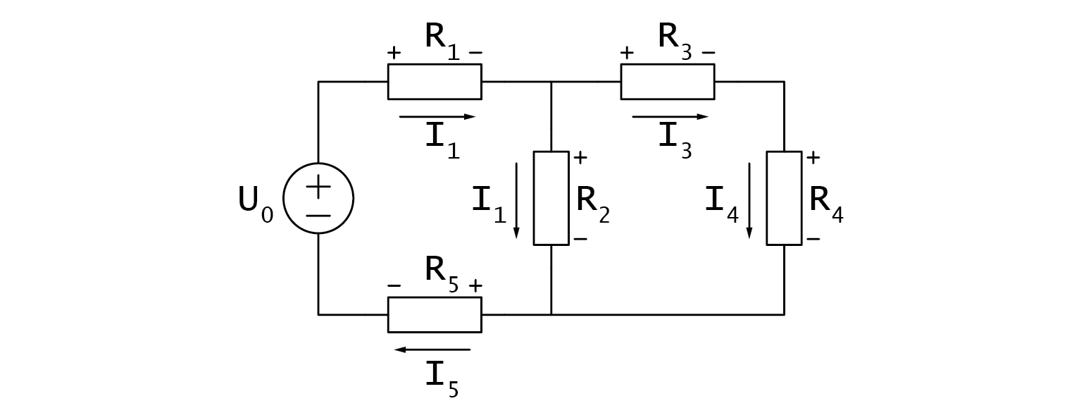
To calculate voltage drop, current, and power dissipation in a circuit, we can use the substitution method to avoid calculating all voltage drops and currents. However, we will now analyze the circuit using a more formal method. The circuit has two branching nodes, so we will need to use two node equations based on Kirchhoff's Current Law (KCL). Additionally, there are three current loops in the circuit, but we will only need to use one loop equation based on Kirchhoff's Voltage Law (KVL).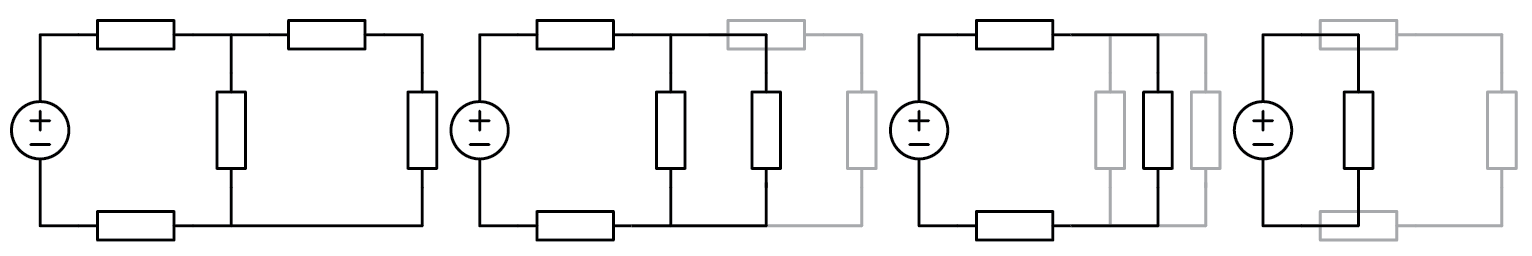
\( I_0=\frac{U_0}{R_{S_{total}}} = \frac{U_0}{(R_1+(R_2 |(R_3+R_4))+R_5 )}=... \)
\( U_{R_2} = U_0 \cdot \frac{R_2 |(R_3+R_4)}{R_{S_{total}}} =... \)
\( I_{R_2} = \frac{U_{R_2}}{R_2} =... \)
\( P_{R_2} = U_{R_2} \cdot I_{R_2}=... \)
It is important to note that our goal of calculating voltage drop, current, and power dissipation in the circuit can be achieved without calculating all voltage drops and currents. However, to analyze the circuit using a more academic method, we must first identify its characteristics. The circuit contains two branching nodes, which requires us to apply two node equations based on Kirchhoff's Current Law (KCL). Furthermore, the circuit contains three distinct current loops, necessitating one less loop equation based on Kirchhoff's Voltage Law (KVL).
Let’s write them down: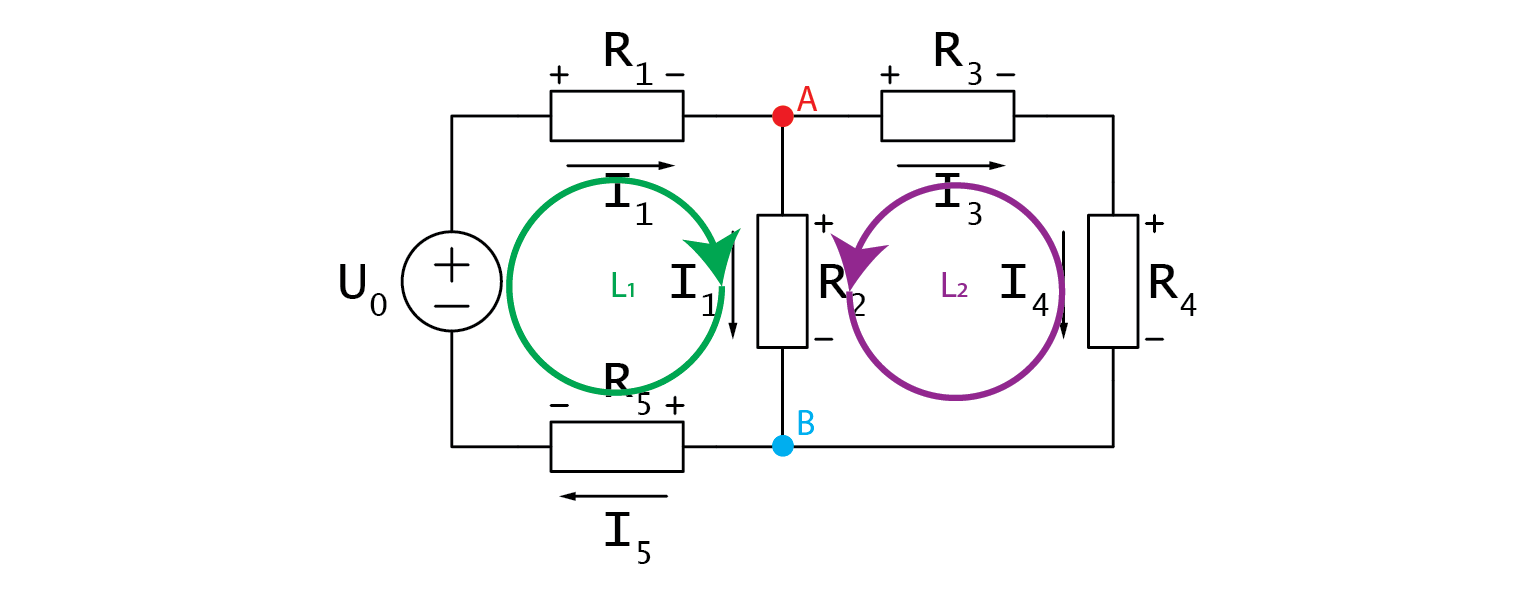
\( A: I_2 + I_3 - I_1 = 0 \)
\( B: I_5 - I_2 - I_4 = 0 \)
I would like to mention that you should immediately see from the schematic that we have redundantly many currents. IS, I1 and I5 are exactly the same, so are I3 and I4 . Moving along the KVL loops, we must be adding any voltage that we hit from the + side, and subtract those that we hit from the - side.
\( L1: \;\;\; U_{R_1} + U_{R_2} + U_{R_5} - U_0 = 0 \)
\( L2: \;\;\; U_{R_3} + U_{R_4} - U_{R_2} = 0 \)
We can utilize the two node equations, based on Kirchhoff's Current Law (KCL), to simplify the analysis of the circuit. Specifically, we can substitute redundant currents in node B with those from node A to simplify the equations.
\( I_5 - I_2 - I_4 = 0 \rightarrow I_2 + I_3 - I_1 = 0 \)
Observant readers will notice that, following this transformation, equations A and B are identical. This simplifies the analysis of the circuit, as we can express one of the currents in terms of the other two and proceed to solve for the voltage equations.
\( I_1 = I_2 + I_3 \)
\( equation\;A \)
Voltage drops in voltage loops should be written as products of currents and respective resistances.
\( U_{R_3} + U_{R_4} - U_{R_2} = 0 \)
\( I_3R_3 + I_3R_4 = I_2R_2 \)
\( I_3(R_3 + R_4) = I_2R_2 \)
\( I_2 = I_3\frac{R_3+R_4}{R_2} \)
\( equation\;B \)
Let's now examine the other voltage loop in the circuit:
\( U_{R_1} + U_{R_2}+U_{R_5}-U_0=0 \)
\( U_{R_1}+U_{R_2}+U_{R_5}-U_0=0 \)
Unlike before, we are dealing with three distinct currents. This can be solved by plugging in Equation A, and we get:
\( (I_2+I_3)R_1+I_2 R_2+(I_2+I_3)R_5=U_0 \)
\( I_2 (R_1+R_2+R_5 )+I_3 (R_1+R_5 )=U_0 \)
\( (I_3 \frac{R_3+R_4}{R_2})(R_1+R_2+R_5 )+I_3 (R_1+R_5 )=U_0 \)
\( I_3=\frac{U_0}{\frac{R_3+R_4}{R_2}(R_1+R_2+R_5 )+(R_1+R_5 ) } \)
And there you go, we now have an equation for I_3 that only relies on known constants. We only need to plug the values in and from there on, dominos will fall. Plugging I_3 into equation B yields I_2. From there on, equation A gives us I_1 and all of a sudden all currents are known. Lastly we can use equation L1 to get any voltage drop we desire and all left to do is to calculate the power, which is now one simple multiplication away. Was this more difficult than doing substitutions? Depends on who you ask. We solved the circuit both ways and you chose the way that best suits you. Besides, the second method yields all voltages and currents at once, which is what you will usually tasked with on the exams.
Hands on
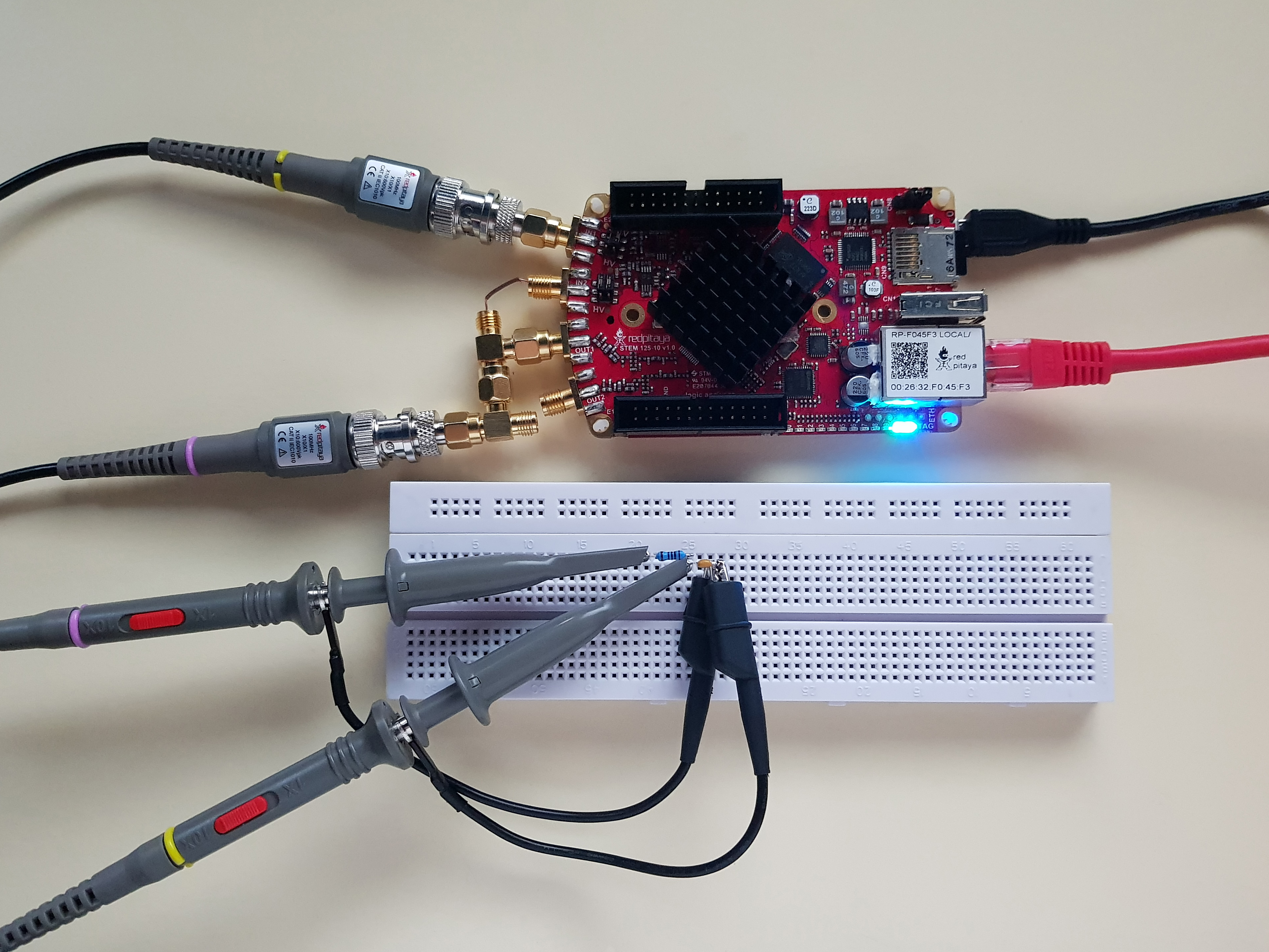
In the context of circuit analysis, it is common to use equations to solve for voltage, current, and power. For this experiment, we will construct a circuit using Red Pitaya and measure the voltage across resistors to test our calculations.
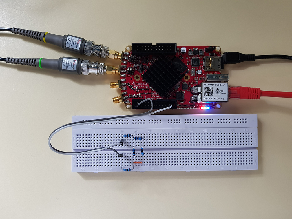
To begin, select resistors with values of at least 100 ohms to avoid any potential damage. Once you have chosen your resistors, build the circuit on a breadboard according to the provided diagram.
Next, choose the voltage source for U_0 from Red Pitaya's supply pins. You have the option to use 3.3 V, 5 V, or even -4 V depending on the requirements of your specific circuit.
After constructing the circuit and selecting the appropriate voltage source, connect probes in 10x mode to Red Pitaya and launch the oscilloscope application. Make sure to set the x10 attenuation in the software as well.
Since we are working with DC signals, it is not necessary to connect the alligator clips, as they are internally connected to Red Pitaya's GND. You can measure voltage on any node by connecting a probe to it.
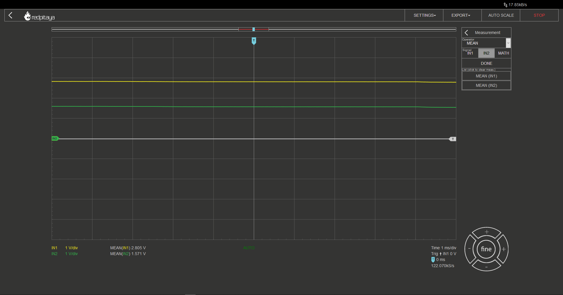
To make reading voltage easier, you may want to set up automatic mean measurements on both channels. This can be done by navigating to the "MEAS" menu and selecting "Operator = MEAN" for each channel, then selecting "DONE." This will display the average voltage for each channel, making it easier to read and interpret the measurements.
I recommend constructing a circuit with no more than three branching nodes to simplify the calculations. Select resistors and connect them in a suitable configuration. Next, use Ohm's Law and Kirchhoff's Laws to calculate the expected voltage drops in the circuit.
To verify the accuracy of the calculations, you can compare the calculated voltage drops with the measured values obtained by using probes connected to the circuit.
Written by Luka Pogačnik Edited by Andraž Pirc
This teaching material was created by Red Pitaya & Zavod 404 in the scope of the Smart4All innovation project.
Transient Response
Transient Response
Objective
The objective of this activity is to inform reader about transient response on a simple circuit that consists of resistors and either capacitors or inductors.Background
It is a well-known fact that in DC conditions, capacitors behave as open circuits and inductors act as short circuits. This assumption is typically made assuming that inductors have no series resistance and capacitors have no parallel resistance, which is often a valid approximation. However, when dealing with time-varying signals, such as when a voltage source is suddenly connected or disconnected, this assumption may not hold true.
To elaborate on the above-mentioned concept, capacitors resist changes in voltage, while inductors resist changes in current. This behavior can be quite useful in certain circuits and applications, and it is important to take into account when designing and analyzing circuits that involve capacitors and inductors.
Capacitors
Capacitors exhibit a characteristic behavior in which they resist sudden changes in voltage, but not necessarily changes in voltage overall. When a voltage is applied to a capacitor, the capacitor will charge slowly over time. Similarly, when a capacitor is discharged, the voltage across it will decrease slowly. However, current flow in a capacitor can change rapidly. This behavior can be mathematically described by the equations:
\( u_C = \frac{1}{C} \int i_c \cdot dt \)
\( i_C = C \cdot \frac{du_C}{dt} \)
In this scenario, we have an R-C circuit that experiences a step change in input voltage from 0 V to \(U_0 \). We can observe how the capacitor behaves in response to this change.
\( u_C = U_0 (1-e^{-t/\tau}) \)
\( i_C = \frac{U_0}{R} e^{-t/\tau} \)
\( \tau = R \cdot C \)
We possess a set of two equations that pertain to voltage and current, respectively, along with a constant denoted by a T-shaped symbol. This symbol is commonly referred to as "tau" and represents the time constant. We will now examine the voltage across a capacitor at various points in time, where time is a multiple of the time constant denoted by the mathematical symbol \(\tau \) .
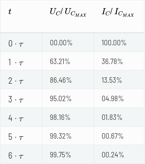
It can be observed that the voltage across a capacitor reaches over 99% of its steady state value after a time interval of 5 times the time constant (5τ), which is why this point is often considered as the final value. Another noteworthy time value is 3 times the time constant (3τ), as the voltage across the capacitor attains exactly 95% of its final level at this point, rendering it easily discernible on an oscilloscope. It is worth noting that the current across the capacitor follows an inverse curve in comparison to the voltage, meaning that the current values can be calculated by subtracting the voltage value from 100%.
Additionally, it should be noted that if the circuit is a CR circuit rather than an RC circuit, the voltage and current equations will be interchanged. Consequently, the voltage across the capacitor will experience a sudden increase, while the current across the circuit will change gradually.
Inductors
We say that inductors resist current change. This works in the same fashion as capacitors resisting voltage change, meaning that current can never change abruptly. The following two equations describe inductor’s voltage and current:
\( i_L = \frac{1}{L} \int u_L \cdot dt \)
\( u_L = L \cdot \frac{di_L}{dt} \)
However, if you are not interested in discussing integrals, and would instead prefer a set of standard procedures or guidelines, then I can assist you with that as well. Let's explore how an inductor behaves when it is subjected to a sudden change in input. For the purposes of this analysis, consider an R-L circuit where the input voltage abruptly increases from 0 volts to a value represented by \( U_0 \)
\( i_L = \frac{U_0}{R} (1-e^{-t/\tau}) \)
\( u_L = U_0 \cdot e^{-t/\tau} \)
\( \tau = \frac{L}{R} \)

Again we have a set of two equations, one for voltage and one for current and one for the time constant. We can now compare capacitor behavior versus inductor behavior and our theory of inductor having an inverse function of capacitor is confirmed.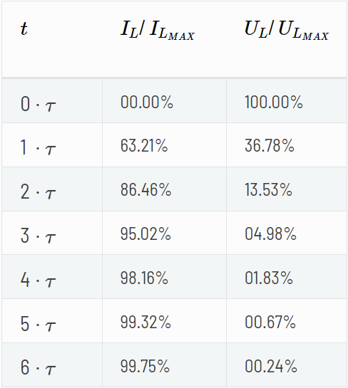
Upon reflection, it appears that the information previously shared regarding capacitors and their behavior has been inadvertently repeated for inductors, with the roles of voltage and current reversed. However, it should be noted that the calculation for time constant tau has been altered. In general, ideal capacitors and inductors are reciprocally analogous, such that only four formulas need to be committed to memory: two for computing the time constant tau, one for a rising signal, and one for a falling signal.
What? Please explain...
Let’s take a look at an example. RC circuit, input voltage drops from 5 V to 3 V ( U_0 =-2 V). Since we are looking at capacitor’s voltage, we should expect that it will slowly drop to that value, meaning that we need to find an equation that will equal 0 at t=0.
\( e^{-t/\tau} \) fits the bill. Final voltage will therefore be starting voltage + voltage change (3 V in this case). Voltage will follow the following curve:
\( u_C = U_{START} + U_0 (1-e^{-t/\tau}) \)
\( u_C = 5V - 2V \cdot (1-e^{-t/\tau}) \)
However, it is advisable to verify this assertion through experimentation, and a red pitaya can serve as a suitable platform for such testing. It is important to note that the voltage range for this setup is restricted to a maximum of ±1 V. With regard to this topic we can move on to our experiment...The experiment
To observe the behavior of a simple RC circuit, it is necessary to connect the probes as follows: Input 1 must be connected to the intermediate node, while the output probe should be connected to the second lead of the resistor. The other lead of the capacitor should be grounded by connecting it to one of the alligator clips. The second input channel should be linked to the Red Pitaya's output. In the video, a Y splitter provided in the Red Pitaya's accessories kit was employed, and a wire was utilized to connect the input and output. Although this method may appear rudimentary, it is the simplest way to accurately observe the output signal. Attempting to measure the signal at the same node as the output probe would be impractical because the probes, which are likely to be employed, contain a 100 Ω internal resistance, even in x1 mode, which acts as a part of a voltage divider. It is worth noting that the second Y splitter was added for the sake of tidiness in the accompanying photograph.
With everything hooked up, you have set input 1 to x10 mode (but input 2 in x1 mode, since it’s just a piece of wire with no attenuation), and set Red Pitaya's signal generator to output a square wave at an appropriate frequency. Appropriate in this case means that it is greater than 1/5τ. I used a 100 Ω resistor and a 10 nF capacitor. Keeping in mind that output probe adds an extra 100 Ω, we get:
\( f_{max}=\frac{1}{10 \cdot 200\Omega \cdot 10nF}=50kHz \)
This will ensure that we can easily observe transient effect without the need to worry about previous transient.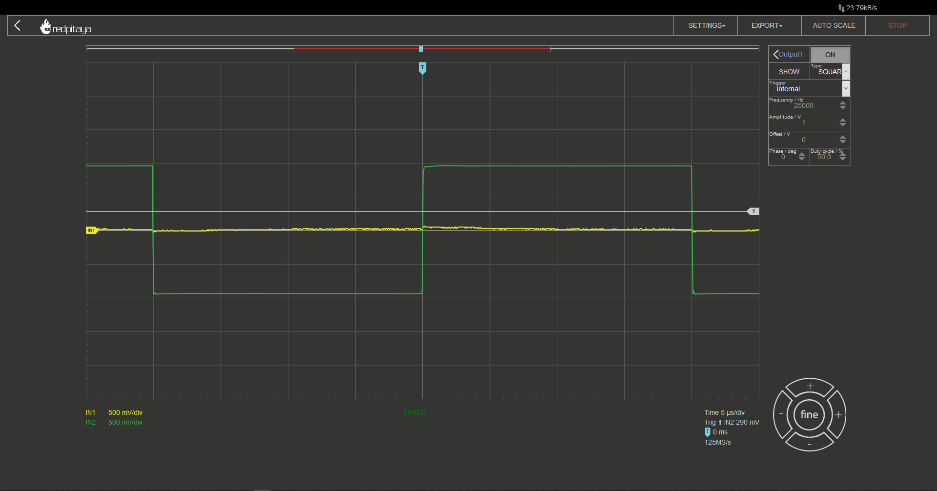
Using cursors, we can measure time for the signal to reach 95% of its change. Since τ = 2 μs we are expecting this measurement to be 6 μs (3τ). Unsurprisingly that is the case. A quick side note: in my case actual peak to peak voltage was 1.85 V, that is why I am measuring time from the start of input change to delta of 1.77 V.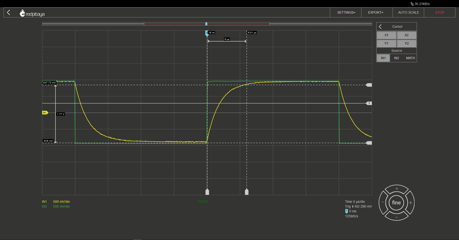
Let’s quickly swap out the capacitor for an inductor. And take a look at the resulting oscillogram.
Here we are measuring the time for voltage to move to within 5% of its final value. 15 μs this time. This is because the inductor I used was, 1 mH and the resulting time constant 5 μs. I encourage you to try making RC and CR circuits but be warned; you will have to use something different than an oscilloscope probe to connect signal generator to the circuit or you will have to deal with resistor divider effect, which will reduce steady state voltage. Here is a photo of a “home lab” setup for such measurement. If you have a proper cable, I encourage you to use it instead. Or just mind the voltage divider and use a standard oscilloscope probe. Not that depicted method is a bit flimsy as cables don’t make the best contact with the signal generator. You might want to press on it.
If you make the experiment, you will notice that CR circuit’s oscillogram takes the shape of RL’s and vice versa. I won’t go into detail about why that is, but I will leave you a hint that it has something to do with capacitors and inductors following their respective current curves, current flowing through resistor and you measuring voltage on same resistors.
One last thing
In the video, a question was posed regarding the outcome of conducting similar experiments on an LC circuit. To answer this query, it is recommended to reduce the frequency of the signal generator and perform the experiment. When conducting this experiment, utilizing a low impedance cable to connect the signal generator to the output would be more effective than using an oscilloscope probe.
It is important to note that the results of this experiment will not be revealed at this time. However, it is possible that the outcome may be useful in a future article.
Written by Luka Pogačnik Editted by Andraž Pirc This teaching material was created by Red Pitaya & Zavod 404 in the scope of the Smart4All innovation project.
Analog Filters
Analog Filters
Objective
The objective of this activity is to introduce reader to the world of passive filter circuits. We will be looking at low pass and high pass filters.
Background
In the previous course, we examined the transient response of simple RC and RL circuits. It was observed that a square wave signal is attenuated when passed through an RC circuit. To ensure this effect, we chose an input signal frequency that had a period longer than the settling time of the RC circuit (5τ). Higher frequencies introduce new complexities such as Fourier analysis. For the purpose of this write-up, we will agree that a square wave signal is comprised of a sine wave at the main frequency and an infinite number of sine waves at odd multiples of the main frequency (3, 5, 7...). An RC filter attenuates these components differently based on their frequency, with higher frequencies experiencing greater attenuation. As a result, the signal's slope is gentler, as observed in the previous course. RC and CR circuits are called filters since they allow some frequencies to pass through while blocking others. It should be noted that this explanation is a simplification, and we will not discuss LR circuits. RL circuits behave similarly to CR circuits, while LR circuits behave similarly to RC circuits. It is also important to note that when discussing signals and frequencies, we are referring to sine wave signals at a particular frequency.
Decibels
Decibels, marked with dB, are a logarithmic unit, used for measuring relative power. To calculate attenuation (or gain) in dB, the following equation is used:
\( G_{dB}=10 \cdot log_{10}(P/P_0) \)If that wasn't confusing enough, it should be noted that decibels are typically used to compare power, but we will be using them to compare voltages. This is possible because we know that power is proportional to the square of voltage, and since exponents inside a logarithm translate to multiplication outside of the logarithm, we can use the following equation:
\( G_{dB}=20 \cdot log_{10}(U/U_0) \)
Simply put, for every 6 dB, signal is multiplied (or attenuated) by a factor of two. For example, 30 dB corresponds 2^5.
Phase
You likely know what happens if we add a fixed value to a sign function: it shifts left/right by a corresponding amount. This shift is known as phase (\( \varphi \) ) .
\( f(t) = A \cdot sin(2 \pi \cdot f \cdot t + \varphi) \)
If \( \varphi \) equals \(\pi \) /2, sine function transforms into a cosine function. If offset value equals 2 \(\pi \) or a whole multiple of that, function is seemingly unaltered.Impedance
Impedance can be thought of as “complex resistance”. It consists of resistance and reactance.
\( Z=R+jX \)
X represents components reactance, which is in complex domain. It is calculated differently for capacitors and inductors:
\( X_C=\frac{1}{2\pi \cdot f \cdot C} \)
\( X_L=2\pi \cdot f \cdot L \)
The j symbol represents complex operator i, because in electronics, lowercase letter i is already reserved for time variable current. Impedance can also be expressed in polar notation as it helps to illustrate attenuation and phase shifting of the signal.
\( Z=|Z| \cdot e^{j \cdot \varphi} \)
\( |Z|=\sqrt{R^2+X^2} \)
Multiplying a signal by \( e^{j \cdot \varphi} \) only shifts its phase by \( \varphi \) without affecting absolute value. This means we can use |Z| to calculate signal attenuation and \( \varphi \) for signal shifting.Background math / complex voltage divider
Aside from the name, there is nothing too complex in the underlying math. Voltage divider, where instead of resistances, we are using impedances.
We can recall that output voltage is caluclated as:
\( u_0=u_i \cdot \frac{Z_2}{Z_1+Z_2} \)When considering only signal attenuation, absolute impedance can be used without complex numbers. This method is similar to calculating resistive voltage divider and only applies to a single frequency, as frequency is necessary for reactance calculation. However, this method does not account for phase shift.
When accounting for different frequencies and phase shift, complex numbers must be used for calculation. Division by complex numbers may be intimidating, but it is necessary for accurate calculations. An example will not be provided for brevity, as this level of calculation is unlikely to be encountered outside of exams.
With the background information covered, the main topic of the course can be discussed.
Filters
All filters have in common the corner frequency. It is also known as a cutoff frequency. This is a frequency at which signal drops by 3 dB, which equals 71% of its initial amplitude \( (1/ \sqrt{2}) \). This frequency is calculated as:
\( f_c = \frac{1}{2\pi \cdot R \cdot C} \)The RC part in the equations presented earlier is denoted by τ, which can be useful in analyzing RL filters.
In simple terms, a low pass filter allows signals below the filter's corner frequency to pass through with no attenuation, and attenuates signals above this frequency at a rate of 20 dB/decade. A decade refers to a range in which the value changes by a factor of ten, such as 1, 10, 100 or 3, 30, 300.
Regarding phase, it begins to shift one decade before the corner frequency and stops moving one decade after it, resulting in a total shift of 90°. The phase crosses the 45° point at the corner frequency.
In reality, signals seldom behave precisely as described above due to various factors. However, engineers use these simplifications as a starting point until the experimental stage of the analysis.
Low pass filter
As mentioned before, a low pas filter is just an RC circuit.
Let’s construct a low pass filter from a 1000 Ω resistor and a 10 nF capacitor. Calculated corner frequency is 15.9 kHz, idealized graph should look a little like this (not that X axis is logarithmic):
In the simplified representation of low pass filters, signal attenuation is presumed to be absent below the corner frequency, while phase begins to deviate one decade before and stabilizes one decade after this frequency. It is important to note that this representation conflicts with the commonly used definition of corner frequency as the point at which signal amplitude crosses the -3 dB threshold, as in this simplified representation, attenuation at the corner frequency is zero. This discrepancy can be regarded as a minor detail of little practical significance.
High pass filter
If low pass is just an RC circuit, high pass filter will probably be a CR circuit.

Let’s take a look at the characteristics of such filter, constructed from same components as before – a 1000 Ω resistor and a 10 nF capacitor. Corner frequency will be the same, 15.9 kHz, but the characteristic curves will be different. Note that the phase axis has been altered.
Bode analysis
The process of measuring the characteristics of a filter in a real-world scenario may raise curiosity. The answer to this question is straightforward: we can excite the circuit with a synthesized sine wave at various frequencies within the desired range and then measure the amplitude gain (or attenuation) and phase shift. Red Pitaya offers a built-in bode analysis functionality, which can aid in this process. To better understand this concept, let us construct a low pass filter and connect it to the Red Pitaya device to observe its behavior.
Hands on experiment
Wiring is important here. If you are ever unsure how to do it, you can always hit “calibrate” button in Red Pitaya’s bode analyzer. Or you can reference this image, that has been taken from RP’s calibration instructions:
It is important to note that the image does not explicitly state that the probes used in this setup must be in x1 mode and the signal output must have the lowest possible resistance. Using oscilloscope probes in place of a cable is not recommended for this purpose. To ensure proper calibration, the "calibrate" button on Red Pitaya's bode analyzer can be used as a fail-safe measure.
With that set, connect to Red Pitaya, click Bode Analyser app and bode plot should start automatically. You can stop it as the default settings are somewhat useless. In settings, set appropriate start and stop frequencies and hit Run. I recommend measuring in at least 100 steps. Once measurement completes, you are left with two curves. Yellow one is for gain, and the green one for phase. Note that gain uses vertical scale on the left, while phase’s vertical axis is on the right. If you want to make measurements, you can add cursors. F cursors will snap to frequency, G to gain, and P to phase. Below is a measurement for a low pass filter, using same components as before:

You will notice that this graph is quite a bit different than the idealized one. There are no sharp corners, corner frequency is too low, phase at corner frequency isn’t -45°, and it never reaches -90°. This isn’t even a comprehensive list of differences between ideal and real bode plot! Some differences can be attributed to idealized graph being oversimplified, some to component values having value tolerances, and some to parasitic properties of used components. Let’s not dwell on that and move on to a high pass filter. Just swap R and C and rerun the analysis.

It is important to note that the image does not explicitly state that the probes used in this setup must be in x1 mode and the signal output must have the lowest possible resistance. Using oscilloscope probes in place of a cable is not recommended for this purpose. To ensure proper calibration, the "calibrate" button on Red Pitaya's bode analyzer can be used as a fail-safe measure.
Written by Luka Pogačnik Edited by Andraž Pirc
This teaching material was created by Red Pitaya & Zavod 404 in the scope of the Smart4All innovation project.
OpAmps 101
OpAmps 101
Objective
The objective of this activity is to introduce the reader to a very useful yet not that well known type of electronic components, the operational amplifiers.
Background
Operational amplifiers, or OpAmps, are electronic components that contain a chunk of doped silicon comprised of several transistors, resistors, and capacitors, hidden within their package. They feature two power pins, two input signal pins, and one output pin. Unlike regular differential amplifiers, OpAmps exhibit very high gain and fast response time, making them suitable for various applications beyond their apparent purpose. These components are configured in a way that results in the output pin producing the voltage difference between the two input pins, multiplied by a significant factor. However, their high gain makes them unsuitable as a differential amplifier.
How it works
OpAmps have two input pins, called inverting (-) and noninverting (+), which should not be confused with the power supply pins. The power supply pins are the positive and negative supply pins, which may be labeled with + and - signs or V+ and V-, and are used to power the OpAmp. OpAmps also have an output pin, and some chips may have additional connections for offset voltage compensation.
It is important to note that the negative supply pin of an OpAmp is not meant to be connected to ground, and the positive supply pin is not meant to be connected to the supply voltage. Instead, OpAmps are typically connected between a positive and negative voltage, with the negative voltage being below ground potential, such as the -4 V pin on the Red Pitaya.
The output pin of an OpAmp is equal to the difference between the noninverting and inverting inputs, multiplied by a large gain factor known as the "open loop gain" (A_OL), which can be as high as 100,000.
\( U_{OUT}=A_{OL} \cdot (U_+-U_-) \)Such a large gain means, that output would exceed supply voltage for even a very small difference between input voltages; even some noise, that gets coupled to inputs, may send the output into saturation. What is saturation? Saturation is what happens when OpAmp’s output hits the limits of how far it can go. And how far is it? Usually from a few volts above negative supply voltage up to a few volts below positive supply voltage. There are some OpAmps who’s output can swing from negative to positive supply voltage. Those are called rail-to-rail OpAmps. And just to make it clear: when OpAmp hits saturation, output gets clamped.
The symbol
OpAmps are available in a variety of package types, but their symbols have been standardized for conveying their functions and for creating electrical schematics for PCB production. The symbol for functional representation does not include power pins, while the schematic representation does. There are additional pins for offset compensation, differential outputs, and other features that are not discussed in this introductory article. It is worth noting that the symbols for OpAmps and comparators are nearly identical, as the two components have similar construction and functions.

Now that we’ve discussed the symbol, it is time to take a look at what can what functions an OpAmp can be used for.
A comparator
Comparators are specialized amplifiers designed to compare two voltages and output a digital signal indicating which input is higher. They are commonly used in applications such as analog-to-digital converters, level detectors, and pulse generators. Unlike op-amps, comparators have a very fast response time and are optimized for speed rather than accuracy.
While comparators can be bought as a separate component, op-amps can also be used as comparators by connecting the output to a voltage rail instead of a feedback resistor. Whenever the voltage at the non-inverting input exceeds the voltage at the inverting input, the output will saturate to the positive rail. Conversely, when the voltage at the inverting input exceeds the voltage at the non-inverting input, the output will saturate to the negative rail. However, it is important to note that comparators have a larger output swing than op-amps and are better suited for high-speed applications.
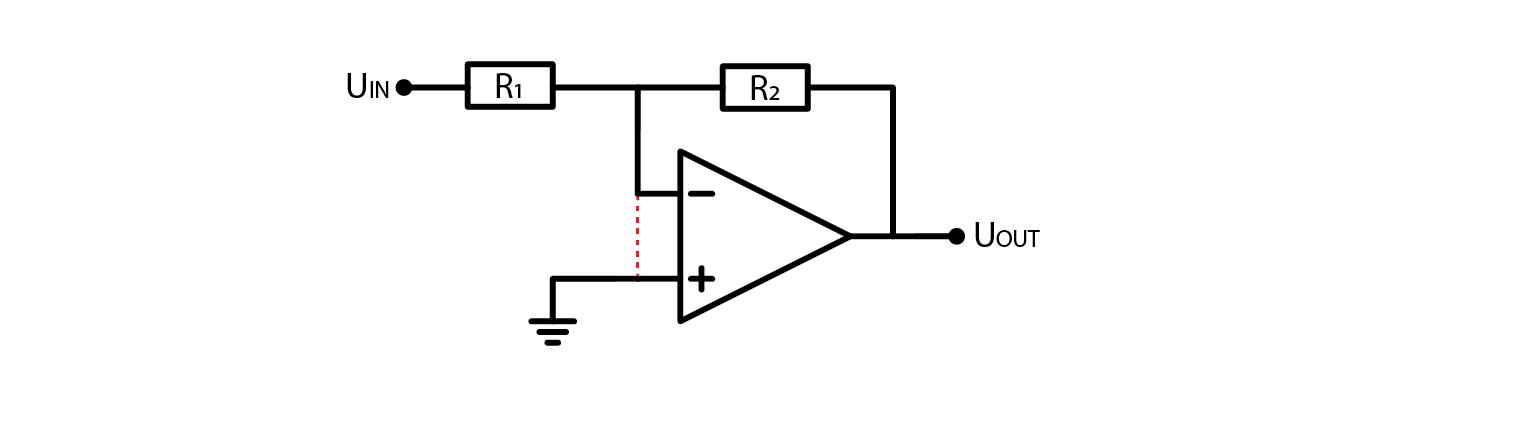
A voltage follower
Let’s make a thought experiment. If we connected OpAmps output to its inverting input, and noninverting input to some arbitrary voltage. What would the output voltage be?

In the previous chapter, we discussed the instability issues when using a comparator instead of an OpAmp. When the output of a comparator is above U+, it hits negative saturation, and when it is below U+, it hits positive saturation. This behavior is not suitable for applications that require stability. In contrast, OpAmps have a slower response time, making them more resistant to becoming unstable. In most OpAmp circuits, when working within voltage limits, the output is equal to the input voltage.
The usefulness of this feature comes from the fact that OpAmps have a large input impedance and a small output impedance. This property allows us to connect OpAmp inputs to any node in a circuit without affecting it, as long as the node's voltage is within the OpAmp's safe operating range. Additionally, we can connect the OpAmp output to any load, as long as the current draw doesn't exceed the OpAmp's rating. This feature is especially helpful in applications such as analog filters, where we want to connect a load to a circuit without affecting it.
An amplifier
Suppose that you desired to amplify the input voltage by a smaller factor, rather than the tens or hundreds of thousands commonly achieved by OpAmps. How would you approach this task?

Let's analyze why this circuit works. Assuming the OpAmp is not saturating, the inverting and noninverting inputs will be at the same potential, which is indicated by a dashed line. It should be noted that the inputs are not physically connected. Now, let's examine the equations:
\( (U_{OUT}-0V) \cdot \frac{R_1}{R_1+R_2}=U_{IN} \)
Resistors 1 and 2 form a resistive voltage divider for output voltage. Obviously Output voltage will have to be greater than input, otherwise original assumption, that both inputs are at the same potential, would be false. If we flip around the equation to express exactly what output voltage should be, we get:
\( U_{OUT}=U_{IN} \cdot (1+\frac{R_2}{R_1} ) \)
Given the equation for the amplifier circuit, it is clear that the output voltage cannot be less than the input voltage if the OpAmp is not hitting saturation. To verify this claim, we can analyze the circuit and confirm that the voltage gain is always greater than or equal to 1.
An inverting amplifier
Given that an OpAmp can be used for signal amplification and has an input called the "inverting input," it follows that there exists a specific circuit configuration called the "inverting amplifier." This configuration is widely used in electronics and serves to amplify an input signal with an amplification factor that is determined by the ratio of two resistors in the circuit. The inverting amplifier is a type of operational amplifier circuit that produces an output that is proportional to the negative of its input.
Once again, starting assumption is that both inputs are at the same voltage. I trust you would be able to derive the formula for output voltage as the approach is the same as before, but if you’ll want to verify your calculations, here is the setup:
\( (U_{OUT}-U_{OUT}) \cdot \frac{R_1}{R_1+R_2}=0V \)
And if we express output voltage as a function of input voltage:
\( U_{OUT}=-V_{IN} \cdot \frac{R_2}{R_1} \)In this configuration, output voltage will always have an inverse sign than input, but its absolute value may be amplified or attenuated. Now that we went through all basic OpAmp circuits, let’s verify that the amplifiers actually behave the way I described.
A non-inverting amplifier - the experiment
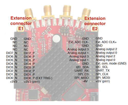
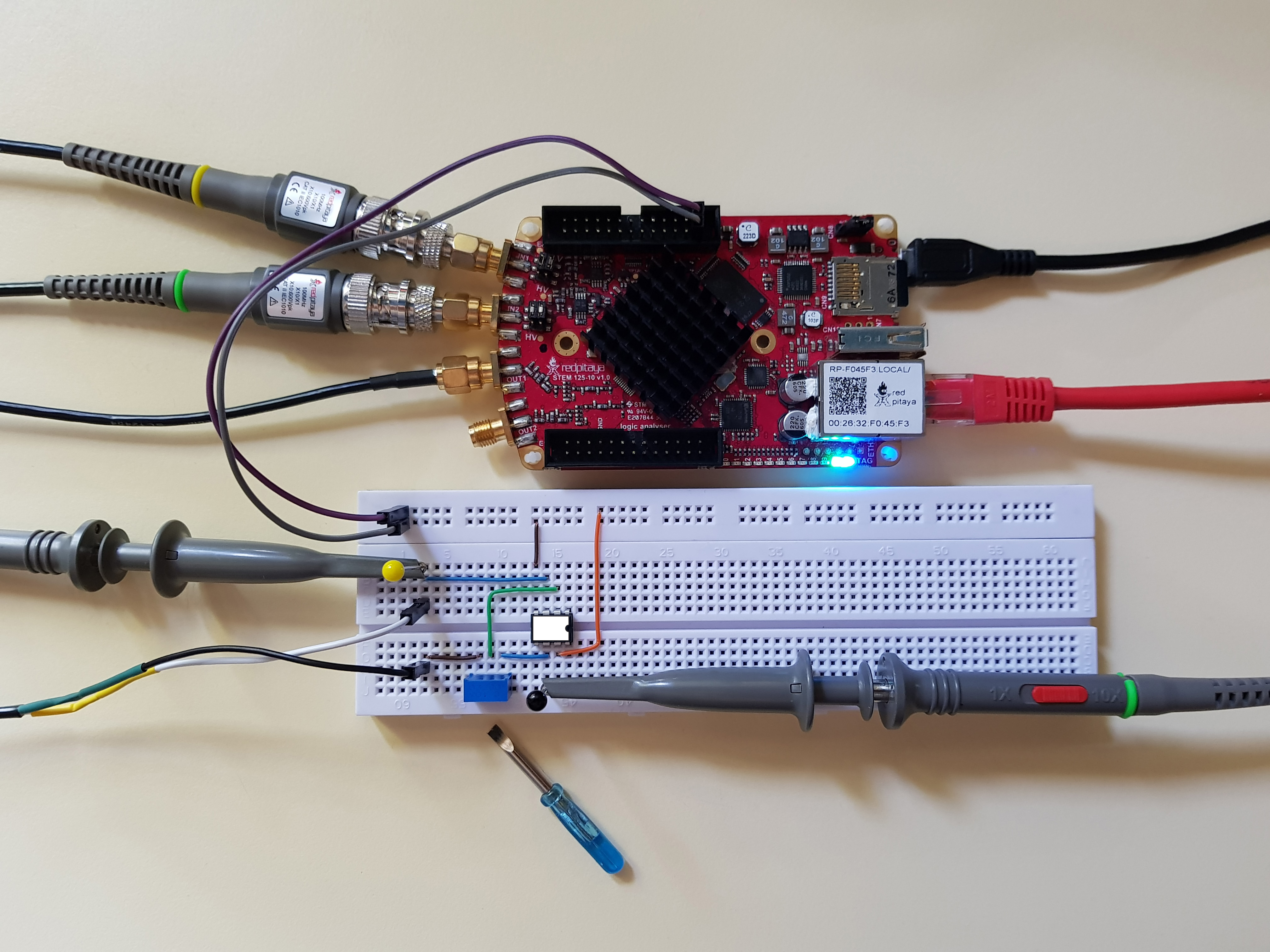
First thing that we will need is an OpAmp. I have decided to use OP37. Why? There are two in the ADALP2000 Analog Parts Kit (the kit this entire set of courses is designed around) so ye can fry one without worrying too much. Here is the chip’s pinout:

Connect U+ to Red Pitaya’s 5V pin and U- to -4V pin. Inputs and output will be connected as per schematic, and the rest (pins with greyed out names) will remain unconnected.
The one difference I made is that I used a potentiometer instead of two separate resistors for R1 and R2. This way I can easily vary resistor ratio. Since this is the most complex circuit so far, I made sure to wire it cleanly so that you can follow the wiring more easily. For those wondering: Connections were made using wires from Ethernet cables. CAT6 works the best. Let’s now connect everything up. All probes in x10 mode, one on input, one on output. Let the Red Pitaya generate a sine wave and connect it to the amplifier’s input. For those playing along at home, I encourage you to turn the potentiometer and observe what happens with the output. What is the maximum amplification? When do you hit Saturation? Are inverting and noninverting inputs really at the same voltage? How about when OpAmp hits saturation? Unfortunately, I can’t show how I turn the potentiometer in this writeup but you can experiment at home, or watch the accompanying video.
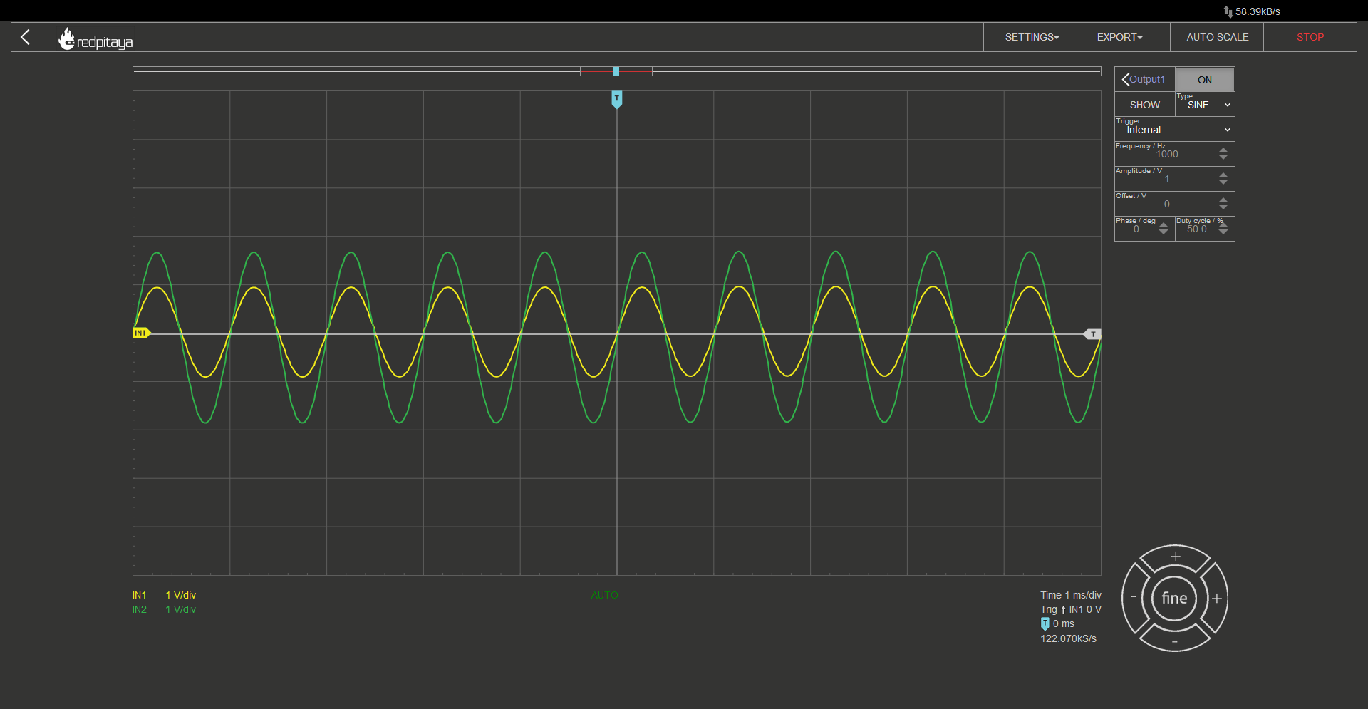
If you followed the diagram correctly, you should see something like this on the screen. At least if you didn’t forget to enable the signal generator and if resistor divider is within what OpAmp can handle.
As a side note I would like to mention that a voltage follower is “just” an extreme variant of an OpAmp amplifier, where R2 equals 0 ohms and R1 is infinite.
An inverting amplifier - the experiment
This experiment will be the same deal as before. I made sure to make the wiring as clear as possible, and used a potentiometer instead of two discrete resistors. Here is the circuit:


I would once again encourage you to see what happens when you turn the potentiometer. Try to make predictions. Maybe measure signal amplitudes and calculate resistor ratio. You can then plug the potentiometer out and measure resistances to verify your calculations.Conclusion
If you read through the entire article, you are now familiar with the four most common (or at least beginner-friendly) applications for operational amplifiers: comparator, voltage follower and two types of amplifiers. If you also followed along with the experiments, you may have gotten a feeling for distortions you will encounter when amplifier is operating close to or beyond saturation. In any case I hope You found this article both interesting and fun. The question I would like to leave you with is: how would you build a noninverting amplifier with attenuation (gain between 0 and 1)?
Written by Luka Pogačnik Edited by Andraž Pirc
This teaching material was created by Red Pitaya & Zavod 404 in the scope of the Smart4All innovation project.
Active Filters
Active Filters
Introduction
In the last two courses we’ve learned about OpAmps and filters. We will be discussing OpAmp filters in this course, which are also known as active filters. We will explore the reasons why OpAmps are used in analog filters and learn how to design them.
The why
Let us examine the effect of attaching a load to the output of a simple RC high pass filter. Although we know how to compute the filter's properties in isolation, attaching a resistive load will inevitably modify the filter's behavior. This is because the newly added load represents an additional resistor in parallel with the filter's resistor. Whenever two resistors are connected in parallel, they can be combined into a single resistor whose resistance is lower than either of the original resistors, which in turn alters the filter's cutoff frequency.

Let’s now take a look at a low pass filter, loaded with a resistive load. The two resistors form a voltage divider, meaning that filter will attenuate even DC signals.

The impact of load on filter performance is more significant when the load impedance is smaller. In contrast, if the load impedance is large, its effect on the filter's characteristics becomes negligible. It is worth noting that the term "resistance" has been used for simplicity, but the same principle applies to capacitive and inductive loads, although their exact impact may differ from that of resistive loads.
OpAmp characteristics
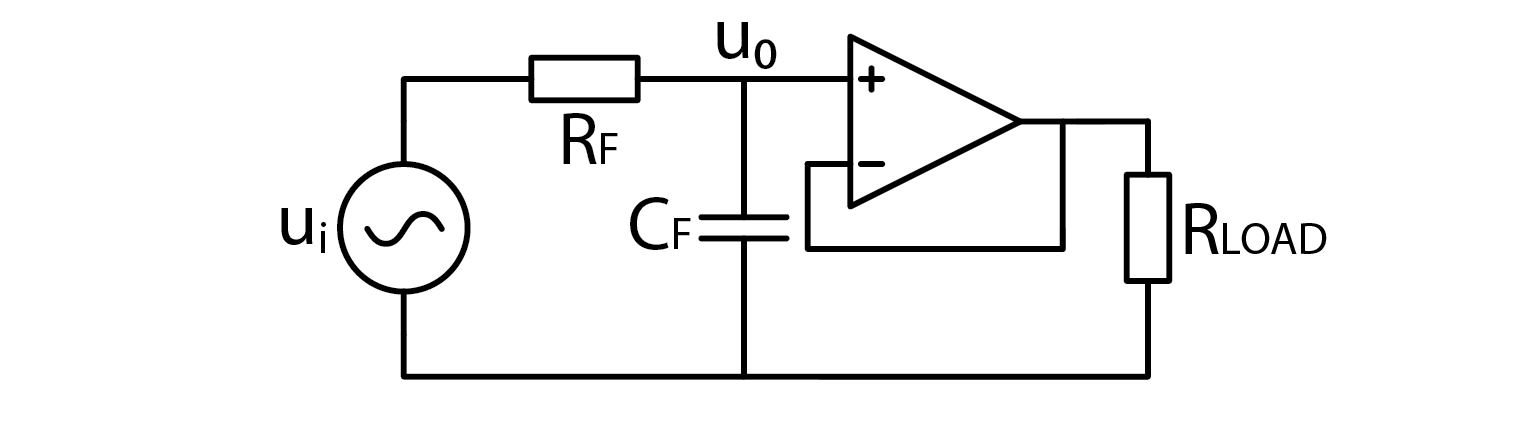
A large input impedance, such as that of an OpAmp, can prevent the load from affecting the characteristics of a filter. By buffering the filter's output with an OpAmp follower, the load is isolated and the filter's behavior remains unchanged. To verify this claim, one can perform calculations or simulations. However, there is an even better solution, which will be presented shortly. The following schematic shows the setup for using an OpAmp buffer:
Second order low pass filter
OpAmp followers are great for buffering regular analog filters, but by adding another RC pair, we can create a second-order low pass filter for even better filtering performance. The detailed explanations of how this works can be found in relevant literature, but here is the schematic:
The perceptive readers may observe a familiar RC low pass filter, followed by an OpAmp follower. However, the remaining part is less straightforward. The cutoff frequency of this filter is computed as follows: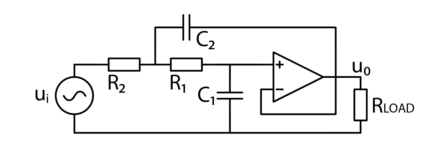
\( f_C=\frac{1}{2\pi\sqrt{R_1 C_1 R_2 C_2 }} \)
Second order high pass filter
The schematic for a second order high pass filter is not surprising, as it is the same as the previous circuit for a second order low pass filter, with the positions of resistors and capacitors switched. The corner frequency is also the same. See the schematic below:

Second order filter benefits
Good question! From what I’ve told you so far, second order filters require an OpAmp and extra pair of resistor and capacitor. Let us explore the benefits of second order filters. The first, and the most prominent one, is greater signal attenuation slope. First order filters’ slope is 20 dB/decade. Each additional order adds another 20 dB/decade, meaning that second order filters have 40 dB/decade attenuation slope. And yes, higher order filters exist as well. Higher order filters also induce more phase shifting. You may recall that standard low pass filter will shift the phase by a total of 90°. This effect is multiplied by the order of implemented filter. This means an ideal second order low pass filter will shift phase by 180° in total.
Band pass filter
We can construct a bandpass filter using the concept of second order filters. However, it's not as simple as combining the components from a low pass and high pass filter. In practice, this approach doesn't work. Instead, we can use an active bandpass filter, which has a different schematic.

This filter has two corner frequencies. One for high pass and one for low pass portion.
\( f_{HPF}=\frac{1}{2\pi R_1 C_1} \)\( f_{LPF}=\frac{1}{2\pi R_2 C_2} \)
One more special thing about this filter is that it is inverting. Negative gain can also be considered as a phase shift of 180°. It is calculated as:
\( A=-\frac{R_2}{R_1} \)
To avoid diving too deep into the mathematical background, let's focus on trying out this filter and observing its behavior to gain a practical understanding.
The experiment
Let’s fire up a Red Pitaya and build the circuit.

You know the drill. Signal generator channel 1 and input channel 1 to filter input, channel 2 to output. Both probes in x1 mode and run the bode analyzer! Both resistors are 100 ohm, the big capacitor (C1) is 47 uF, the small one is 100 nF, and here is what I got:

Nothing too special, sure, but we can move cutoff frequencies to alter the filter’s characteristics. This can be done either by changing resistors or changing capacitors. The following bode plot shows filter’s characteristics where C1 or R1 got changed by a factor of 10. I will let the reader try to determine which component got changed. Hint: take a look at the Y axis.

Conclusion
You can play around with the other two active filters we discussed in this course as well but I won’t take any more of your time. Hope you learned something new, if nothing else, that a voltage follower can be used to make sure load doesn’t affect signal shape.
Written by Luka Pogačnik Edited by Andraž Pirc
This teaching material was created by Red Pitaya & Zavod 404 in the scope of the Smart4All innovation project.
Superposition
Superposition
Introduction
Because I know that you’ve more than likely had enough of all the OpAmps and filters and OpAmp filters and such, we will be making a break from all those fancy circuits and components, and focus on the basics. We will take a look at a trick, that can be used with linear circuits with multiple voltage or signal sources, the superposition.
But why?
The answer is simple. Take this very simple circuit and tell me, what current flows through, let’s say… R2?

Even though this circuit consists of mere five components, solution is all but trivial. In the first course I showed you how to simplify a simple resistive circuit, but this doesn’t work here as we have two voltage sources. The only way to solve this circuit is by good old fashioned calculations. Let’s start with the two nodes.
\( A:-I_1+I_2-I_3=0 \rightarrow I_2=I_1+I_3 \)Ok, this wasn’t so bad, how about the loops?
\( L1 \)
\( U_{R_1}+U_{R_2}-U_1=0 \)
\( I_1 R_1+I_2 R_2=U_1 \)
\( I_1 R_1+(I_1+I_3 ) R_2=U_1 \)
\( I_1 (R_1+R_2 )+I_3 R_2=U_1 \)
\( I_3=\frac{1}{R_3} (U_1-I_1 (R_1+R_2 )) \)
\( L2 \)
\( U_{R_3}+U_{R_2}-U_2=0 \)
\( I_3 R_3+(I_1+I_3 ) R_2=U_2 \)
\( I_3 R_3+(I_1+I_3 ) R_2=U_2 \)
\( I_1 R_2+I_3 (R_2+R_3 )=U_2 \)
\( I_1 R_2+\frac{R_2+R_3}{R_3} (U_1-I_1 (R_1+R_2 ))=U_2 \)
\( I_1 (R_2-\frac{(R_2+R_3)(R_1+R_2)}{R_3})=U_2-\frac{R_2+R_3}{R_3} U_1 \)
\( I_1 = \frac{U_2-\frac{R_2+R_3}{R_3} U_1}{R_2-\frac{(R_2+R_3)(R_1+R_2)}{R_3}} \)
Luckily this is all we need. Let’s say that all resistors were 100 ohms, U1 was 5V and U2 was 3.3V. Plugging those numbers in above equations we get the following resistor currents:
\( I_1=22.3 mA \)
\( I_2=27.7 mA \)
\( I_3=5.3 mA \)
Since all resistors are a hundred ohms, the voltage drops on resistors are just current through a resistor times one hundred.
A better alternative
If you skipped all the calculations in last chapter, I can’t blame you. They were everything but fun. And that was for a very simple circuit with two voltage sources and three resistors, just think what would happen if we had any more components! Luckily there is a better way. We call it superposition. If a circuit is linear (this means that output can be written in the form of a \cdot U_1+b \cdot U_2+...+x \cdot I_1+y \cdot I_2+...=X), we can analyze the circuit with only one source connected at a time. We do that for all sources and sum up the results to get the full output. This is known as superposition. Note that “disconnection” means a different thing for voltage and current source. Voltage source gets replaced by an open circuit, while a current source is replaced by a short circuit as depicted below.

Let’s see how one would apply superposition theorem on this circuit. First, let’s disconnect U2 and solve the resulting circuit. Mind the direction in which currents are flowing as this is very important.
\( I_{1_{(1)}}=\frac{U_1}{R_1+R_2 |R_1}=\frac{5 V}{100 \Omega+50 \Omega}=33.3 mA \)\( I_{2_{(1)}}= -I_{3_{(1)}}=\frac{I_{1_{(1)}}}{2}=16.7 mA \)
When U1 is disconnected we get the following:
\( I_{3_{(2)}}=\frac{U_2}{R_3+R_1 |R_2}=\frac{3.3 V}{100 \Omega +50 \Omega}=22 mA \)
\( I_{2_{(2)}}= -I_{1_{(2)}}=\frac{I_{3_{(2)}}}{2}=11 mA \)
And to get the final result it up:
\( I_1=I_{1_{(1)}}+I_{1_{(2)}}=33.3-11=22.3 mA \)
\( I_2=I_{2_{(1)}}+I_{2_{(2)}}=16.7+11=27.7 mA \)
\( I_3=I_{3_{(1)}}+I_{3_{(2)}}=-16.7+22=5.3 mA \)
If you ask me, this method is a lot better. Much simpler. Harder to get wrong. Add more positive descriptors.
The expereiment.
There is always an experiment. But this one will be extra simple. Build a circuit and learn how to efficiently measure it. 5V, 3.3V, and GND are stolen from the Red Pitaya and both probes are set to 10x mode.

Since this is a DC circuit with no AC stimulation, channels 1 and 2 will be just straight lines, effectively acting as voltage meters. Voltage drop between nodes can be automatically calculated by selecting MATH->Operator = “minus“->ENABLE. It would also be wise to add automatic measurements on all signals by clicking MEAS->Operator = “MEAN” ->DONE. Do this for all signals, IN1, IN2, and MATH. You can now play around with analyzing this circuit. Or maybe you would like to build a fancier one and play around with it. Red Pitaya has one more voltage output pin, -4V, hint hint…

Conclusion
Superposition is a powerful tool for analyzing linear circuits. Whenever possible, it will be an easier alternative to “standard” calculations. Disconnect all but one source, calculate whatever you want to calculate, rinse and repeat for other sources. We will explore a practical application of superposition in next course.
Written by Luka Pogačnik
This teaching material was created by Red Pitaya & Zavod 404 in the scope of the Smart4All innovation project.
Analog Addition and Subtraction
Analog addition and subtraction
Introduction
In this course, we will dive into the fundamental concepts of adding and subtracting using operational amplifiers (OpAmps). These concepts serve as the building blocks of arithmetic operations, and their understanding is essential to comprehend more advanced electrical circuits. While we have covered voltage dividers, multipliers, and inverters, which involve mathematical operations such as multiplication and division, the focus of this course will be on the basic algebraic operations of addition and subtraction. We will demonstrate how OpAmps can be employed as effective tools for implementing these operations in electrical circuits.
Addition
In primary school you learned to add numbers before subtraction, and we will follow the same steps here. Addition first. We want a circuit that will be able to implement the following function:
\( U_{out}=a \cdot U_1 + b \cdot U_2 \)To make things easier to understand, let’s first take a look at how we would implement just one part of this equation, \( U_{out}=a \cdot U_1 \) for example. One circuit that matches this equation would be an inverting amplifier.

It implements the function \( U_{out}=-\frac{R_2}{R_1} \cdot U_1 \). Now let’s make a thought experiment. If we added another voltage source, U2, connected to the inverting input of OpAmp through a capacitor, and U2 was at zero volts… What would happen? Output voltage wouldn’t change since inverting input is a virtual ground. But if we set U1 to 0V and U2 to something different, implemented function would be \( U_{out}=-\frac{R_2}{R_3} \cdot U_2 \).

Did you read the previous course on superposition? If you did, you must have already guessed what direction we’re heading. Superposition. Function \( U_{out}=a \cdot U_1 + b \cdot U_2 \) is a textbook example of a linear combination of multiple inputs, making it suitable for solving with superposition theorem.
We have acquired knowledge on how to add two voltage sources together using operational amplifiers (OpAmps). However, it should be noted that this principle can be extended to include any number of additional voltage sources. By connecting these voltage sources, each with their respective resistor, to the inverting node of the OpAmp, the resulting function will remain consistent with expectations. This demonstrates the versatility of OpAmps and their ability to add an indefinite number of voltages.
Addition experiment
To validate the principle of adding an indefinite number of voltage sources using operational amplifiers (OpAmps), it is recommended to perform an experiment using a Red Pitaya. While the Red Pitaya has only two outputs, one can still implement a simple inverting adder circuit for two inputs. To expand the circuit to include additional signals, one can introduce external voltage sources or even add a voltage divider to generate a customized voltage level. This experiment will help to confirm the validity of the principle and demonstrate the versatility of OpAmps in adding multiple voltages (for the sake of simplicity of this experiment you can use our 3.3V ,5V and -4V pins, so you don't have to deal with the voltage devider).

Setup is the same as usual. Input probe in 10x mode, both in hardware and in software. All resistors were 1 kOhm. The following Screencapture is with both output channels enabled, one is outputting a sine, and the other a square wave function. I will let you decide of the output function, yellow, is a, inverted sum of the two inputs.

Having established the functionality of an inverting adder circuit using operational amplifiers (OpAmps), the task at hand is to design a noninverting adder circuit. However, it is crucial to note that connecting two inputs directly can lead to a short circuit, and potentially damage the Red Pitaya. To avoid this, resistors should be introduced, with a recommended value of 1k or preferably 10kOhm. The circuit can be built using a noninverting amplifier and taking advantage of superposition. It is worth mentioning that an inverter should not be added to the output to achieve the desired functionality.
Subtraction
The concept of subtraction can be boiled down to the inversion of the second operand and addition of the two operands. To achieve this in an electrical circuit, a combination of inverting and noninverting amplifiers can be employed, much like in the case of addition. However, it is worth noting that using a dedicated inverting amplifier to invert one input voltage is not the most elegant approach. Instead, we can adopt a more sophisticated solution, which involves the use of the following technique:

The U2 branch of the circuit is relatively straightforward. When U1 is set to zero, the circuit behaves similarly to a standard inverting amplifier. However, when U2 is set to zero, the analysis becomes more complex. It is essential to remember that during normal operation, the inputs of the OpAmp are at the same voltage. As a result, we get the following two equations:
\( U_+=U_1 \cdot \frac{R_4}{R_3+R_4} \)
\( U_-=U_{OUT} \frac{R_1}{R_1+R_3} \)
When we combine them, we get:
\( U_{OUT}=U_1 \frac{R_4}{R_2+R_4} \frac{R_1+R_3}{R_1} \)
The circuit functions as a nonstandard noninverting amplifier, and while it may deviate from the standard approach, the equations derived from its analysis are still valid. By selecting components such that R1 is equal to R2, and R3 is equal to R4, we can simplify the equation to the following form:
\( U_{OUT} = \frac{R_3}{R_1}(U_1-U_2 ) \)
The circuit above is commonly known as a differential amplifier.
Differential amplifier experiment
Let's connect the OpAmp in differential orientation to Red Pitaya as shown in the picture bellow, so we can watch what happens to our input signal, when driven through the differential amplifier.

Same as before, probe in 10x mode, one output is sine, the other square wave, all resistors are 1k, and this is the result:

Conclusion
By combining the concepts of inverting and noninverting amplifiers, we have successfully demonstrated the implementation of all basic arithmetic operations in analog circuits. This includes addition, subtraction, multiplication, and division. The latter can be achieved either by using resistors to divide by a constant or by multiplying with an inverse number to divide by an arbitrary value. Although there also exists a circuit for arbitrary division, we will not go into further detail on this topic. I hope that you found this course engaging and informative, and that you have gained valuable knowledge and skills from it.
Written by Luka Pogačnik Edited by Andraž Pirc
This teaching material was created by Red Pitaya & Zavod 404 in the scope of the Smart4All innovation project.
Diodes
Introduction
Throughout the courses, we have primarily dealt with components that are nonpolar (polarity agnostic), meaning that their orientation does not affect their behavior. However, the component we will be exploring today is vastly different in that its characteristics are highly dependent on its polarity. This component is none other than the diode.
What is a diode?
Diode is a semiconductor component that allows current to flow in one direction, but prevents it from flowing the other way. How? Diodes consist of doped silicon. One part is doped to be positive (P) and the other to be negative (N). When P and N doped silicons contact, they form a PN junction. This junction exhibits a strange phenomenon: current can flow in direction from P to N but not in reverse. This has to do with energy levels in atoms and we won’t go into details.
Different kinds of diodes
Diodes are available in several types. The most common is the classic diode, which has no special properties. Schottky diodes are similar to classic diodes, but they have a lower forward voltage, making them suitable for faster switching. These diodes are commonly used in SMPS power supplies. Zener diodes are regular diodes, but they have a very steep reverse breakdown voltage when they are polarized in the reverse direction, making them a good voltage reference. The exact voltage can even be selected during manufacturing, making them even more useful. Lastly, we have light-emitting diodes, commonly known as LEDs. These diodes function like regular diodes, but emit light when current flows through them in the forward direction. Although there are a few more types of diodes, we will limit our discussion to these in this course.

Markings
As mentioned before, polarity of diodes is important. P and N parts have special names. Positive end is called anode, and the negative is called cathode. If you have trouble remembering this, try the acronym PANK (misspelled punk, Positive Anode Negative Cathode). Diodes come in different shapes and sizes. In the days of THT (through hole technology), cathode was marked with a straight line (resembling the line at the end of the arrow on the electrical symbol). This usually still holds true with SMD components. Other option for marking diodes polarity, very common with LEDs, is making the cathode by making its lead shorter. The following photo shows three different diode packages, all are oriented such that anode is at the top and cathode at the bottom.

Forward voltage
Diodes conduct current only in forward direction, but current Vs. voltage characteristic follows an exponential curve. This means they are very lousy conductors at low voltages and very good conductors at high voltages. To simplify calculations, engineers came up with the following simplification: let’s say that voltage drop on a diode is constant and ignore its IU curve altogether.

Using this, we can calculate current through a simple resistor – diode circuit as such:
\( I_D=\frac{U_0 - U_F}{R} \)Forward voltages are different for different diodes. Standard diodes have 0.7 V, Schottky diodes can go down to 0.3 V, and LEDs have 1.6 V for classic red ones or more. Blue white and UV LEDs can easily exceed 3 V.
Reverse breakdown voltage
Diodes conduct current only in forward direction, but that is a simplification. They really conduct a bit of voltage in reverse direction. Total conducted current is quite small and more or less constant, regardless of applied voltage, but beyond reverse breakdown voltage, current increases exponentially. Zener diodes exhibit especially steep characteristic, making them suitable for being used as voltage references.
Diode experiment
Let’s make a very simple circuit and measure the output. You know the drill. Input at 10x, output should be a sine wave, +- 1 V. The diode I used in my experiment was 1N4001¸, one of the most classic diodes known to man.


At vertical resolution of 0.5 V/div you can see that green line (after diode) is always equal or greater than 0 V but also approximately 0.7 V less than the yellow line (function generator). Exactly the forward voltage. But this was a very simple experiment and we haven’t mentioned OpAmps yet. Let’s try measuring currents through different diodes at higher voltages.
LED experiment
Here is what we are about to do: Red Pitaya can only output +- 1 V, but we want to test LEDs. Because LES’s forward voltages exceed RP’s output range, we have to extend it. My proposed solution is a noninverting amplifier with x3 setting. Schematic and the corresponding circuit are depicted below.

The 100 ohm resistor serves two purposes: first, it limits the current to prevent damage to the diode, and second, it functions as a shunt resistor to enable measurement of the current.

Signal generator outputs a triangular waveform at 1 V amplitude. Probes are in 10x mode and connected to the 100 ohm resistor. I also added a math function to calculate the difference between the first and the second probe. This corresponds to the current flowing through limiting resistor and the diode. Actual current is voltage drop divided by resistance. Before showing the results, let’s discuss the power supply for OpAmp. It is powered form RP’s 5 and -4 V pins. Output voltage will try to swing from -3 to +3 V, and the negative power supply won’t allow that, as clearly seen on the oscillogram below:

Yellow is RP’s output voltage, and green is amplified voltage after the noninverting amplifier. Clipping is visible but that fortunately doesn’t concern us as no current will be flowing in that phase. And now, some results. Green trace is before shunt resistor, yellow one is after it, and the purple one is their difference. The two dashed horizontal lines depict the point where current starts flowing (bottom) and the forward voltage (top).
Red LED:

Green LED:

White LED:

We can clearly see that peak current is getting lower and lower with each graph. Red has highest current rating and white has the lowest one. That is inversely proportional to forward voltage, which is the greatest for the white LED. Can you find a reason for that phenomenon? Let me give you a hint. Red has the longest wavelength (lowest frequency) of the bunch, green has shorter wavelength (higher frequency), and so on. Higher frequency means higher energy. Was that helpful enough? White LED is based on blue or ultraviolet (UV) diode, and we see its forward voltage in the last oscillogram. Can you predict forward voltage of an infrared (IR) LED? If not, you can always make an experiment. You have one IR LED in the ADALP2000 kit. It’s one of the black looking diodes – the one that is slightly translucent with a bluish tint.
Extra credits
Throughout this course we observed characteristics of single diodes. Can you find a way to measure the characteristics of multiple equal or different diodes, wired in series using only a Red Pitaya and nothing else?
Conclusion
So this was a quick introduction to LEDs, I hope you fund it enlightening. At least the experiment with LEDs. Jokes aside, when you encounter the next problem, when you will want the current to flow in only one direction, or when you want to use an LED with an appropriate current setting, you now know how.
Written by Luka Pogačnik Edited by Andraž Pirc
This teaching material was created by Red Pitaya & Zavod 404 in the scope of the Smart4All innovation project.
Full Wave Rectifiers
Full wave rectifiers
Introduction
The national electrical grid provides an abundance of electricity to users in the form of alternating current (AC) at 110 to 230 volts and 50 or 60 Hz, depending on the region. However, what if someone requires a continuous supply of direct current (DC) voltage from this source? This course will cover full wave rectifiers, which are commonly used in the industry for converting AC to DC.
What is a full bridge rectifier?
In the last course we covered a half wave rectifier – just a simple diode. When AC voltage is applied to its anode, cathode will conduct only during the positive halfwave. Resulting waveform is far from DC, but it is always positive. If averaged the output, we would get a DC voltage source. This method has many significant drawbacks. Most of them originate from the fact, that diode is in conducting mode for only about half the time, but we won’t go into details. Finding a circuit, that will conduct voltage in positive direction would alleviate the problem. Conveniently such circuit exists and is depicted below. We call it a full wave rectifier.

A full wave rectifier is composed of two pairs of diodes that ensure voltage 'flows' in the correct direction. It converts AC voltage to DC voltage. To comprehend its operation, it is useful to examine what happens when the applied voltage is positive and negative. For the purpose of analysis, we can assume that diodes conduct electricity when the current flows from the anode to the cathode.

If we apply a signal to an ideal full wave rectifier, its output will be an equivalent of mathematical function out=abs(in). To illustrate that with a sine wave input where black is input and red is rectified output:

The experiment
Without further ado, let’s build a full bridge rectifier and try it out. Let Red Pitaya output a +-1 V sine wave for an input signal, and connect one probe to the input and one to the positive output as depicted below. Note that I used the alligator clip on output signal this time.

Aside from a bunch of seemingly useless wires to the left, which I call foreshadowing, I added a 1 kOhm load resistor to the output. I will let you experiment what happens without one. Anyway, the signal output is such:

No, this is not a wrong screencap, this waveform is correct. Correct but not desired. First let’s point out that waveform resembles a half wave rectifier. Second let’s discuss the voltage drop. A real diode rectifier will always have some voltage drop. The exact value can be estimated. You may recall from the previous course, that diodes usually have 0.7 V drop. That is the case for the diodes I used as well. What you can see from the screencap is that the voltage drop isn’t 0.7 V, it is closer to 0.6 V. You may say this is nothing special, 0.6 is very close to 0.7. Yes, I agree, but since current flows through two diodes, voltage drop should be 1.4 V. What’s up with that? The explanation is very simple. Red Pitaya can only output +-1 V signal, which is less than a nominal voltage drop on a pair of diodes. This means that diodes are operating below the point where we can simplify their characteristic to a simple voltage drop, which explains the unexpected voltage drop. And what explains the half wave instead of full wave rectifier characteristic? This has nothing to do with diodes, and all to do with Red Pitaya. By connecting the alligator clip to the negative output of a full wave rectifier, we effectively shorted half of the rectifier, ruining the characteristics. Resulting circuit looks like this:

So this is actually just a half bridge rectifier with a short circuit to ground when input is negative... Wait, does that mean that what I told you about expected voltage drop being 1.4 V was wrong? Yes, but I wanted to share a glimpse into how troubleshooting works. Find an explanation and work with it until you can prove it doesn’t work. What happens if you don’t connect a grounding clip can be considered your optional homework, because solution lies elsewhere and I don’t want to drag this article too long.
A transformer.
There are only a few devices that require rectified mains voltage to operate. Usually required voltage is a lot lower. A low cost solution is to use a transformer with an appropriate winding ratio. A transformer outputs voltage that is higher, lower, or equal to the input voltage based on how many turns input and output windings have. The exact relation is such:
\( U_{OUT}=\frac{N_OUT}{N_IN} U_IN \)Aside from changing the amplitude, a transformer also galvanically disconnects input and output. ADALP2000 component kit, from which we select components for this course, has two transformers in it. Both are from Coilcraft’s Hexa-Path series. They have six individual windings, from which we can construct “any” transformer we want. Biggest voltage ratio we can construct is 5:1 (or 1:5). This is done by selecting one coil to be input/output, and wiring the remaining five in series, paying attention on polarity (marked with a dot next to the inductor symbol. The following diagram is from the transformer’s datasheet

Consumer electronics usually use a transformer to convert mains voltage into something lower, but we will be using it in reverse: to change RP’s +-1 V output to +-5V. Here is input to the transformer in such configuration (yellow) Vs. output (green).

A full wave rectifier with a transformer
With all that said, let’s construct such circuit:

Aside from the transformer, everything is exactly the same. Even those wires I called foreshadowing are in exact same spots. As if someone showed you exactly how to connect transformer’s windings to achieve 1:5 winding ratio… Anyway, here’s the setup:

Note that you have to set Red Pitaya’s signal generator to output a sine wave at a high enough frequency. Transformer’s inductance is very low in comparison to transformers used in household appliances, thus frequency has to be a lot higher. I found 100 kHz to work fine. Te transformer I used was HPH1-019L. Here is what I got:

All as expected. Rectified output’s peak voltage is 5x input minus two diode drops. But I opened this course up by talking about DC power supplies… this means I have to show you how to smooth this voltage!
A DC power supply
Let’s summarize what we now know how to make: We know how to change input AC voltage’s amplitude by any desired factor by selecting appropriate transformer coil winding ratios, and we know how to convert AC voltage to one that oscilates between 0 and V_{IN}-2 \cdot V_{DIODE}. All that is left to do is to average this out. One way would be to use an RC filter. A great downside to this approach is that all current that a powered device consumes has to flow through the filter’s resistor. This leads to great power losses. A smarter solution is to use an LC filter, which behaves similar to two RC’s in series (I won’t go into details), where the L part is the transformer itself! Capacitor is wired between output’s + and – nodes. Depending on its capacitance, we get different results. Here is output voltage with a 10nF capacitor:

And here is one with a 47 uF capacitor:

We can clearly see that bigger capacitance leads to better smoothing. Another thing you can see is that input voltage’s shape gets distorted. That is because voltage source gets overloaded.
Conclusion
This concludes our quick intro to full wave rectifiers and their applications in simple and cheap power supplies. Note that output voltage of such power supply is unregulated. This means that an additional regulation is often needed. I encourage you to test how output voltage varies with different loads. Can you guess what would happen if load was removed completely? I hope you learned something.
Written by Luka Pogačnik Edited by Andraž Pirc
This teaching material was created by Red Pitaya & Zavod 404 in the scope of the Smart4All innovation project.
- This topic
Schmitt Triggers
Schmitt triggers
Introduction
Comparators are electronic devices that are commonly used in circuits to compare two voltage levels. When the voltage level at the noninverting input is greater than that at the inverting input, the output of the comparator is driven to positive saturation. Conversely, when the voltage level at the inverting input is greater than that at the noninverting input, the output is driven to negative saturation. However, if the voltage levels at the inputs are very close, the output can become unstable and oscillate between the two saturation voltages, especially if the noninverting input is subject to noise. To overcome this issue, a deadzone can be introduced, which prevents the comparator from toggling its output when the input voltage changes within a certain range. This helps to improve the stability and accuracy of the circuit.
Comparators
Let’s start this course off by refreshing our knowledge about comparators. They are essentially OpAmps that sacrifice their stability for faster switching speed. Much in the same way as OpAmps, their output is the voltage difference between noninverting and inverting inputs, multiplied by a huge factor.

For almost any real application, their characteristic can be described as such:
\( U_{out}= U_{sat+} \; when \; U_{+} > U_{-} \)
\( U_{out}= U_{sat-} \; when \; U_{+} < U_{-} \)
Depending on which input (inverting or noninverting) we select to be reference input, we can obtain an inverting or a noninverting comparator as shown on the image below.

Modifying a comparator
Now that we have a fundamental understanding of comparators, let’s conduct a simple experiment using an inverting comparator with the OP37 chip. We will power the OpAmp from a symmetrical +-3.3 V source instead of the usual +5 -3.3 V source. To conduct the experiment, we will set one of Red Pitaya’s outputs to output a DC voltage as our reference voltage, and the other output will generate a sine wave at the maximum amplitude as our input signal. By connecting one input probe to the comparator’s output and the other to the sinusoidal output, we can observe the output behavior as we modify the circuit. As expected, the output will be negative when the input is greater than the reference, and vice versa. I encourage you to follow along as this is a very straightforward experiment.

What would happen if we added a load resistor to the comparator’s output? Nothing. Probably because you forgot that the loads resistor has to be connected to the ground. But even if you connected the load resistor as one should, you should still see that the output voltage remains unchanged. Unless the resistor was very small and you would overload the comparator’s output stage. Now what would happen if we replaced this one resistor with a pair of them wired in series? And let’s make them a potentiometer so that we will be able to vary their ratio easily. Unsurprisingly, comparator’s output remains unchanged. From the comparator’s perspective a potentiometer is exactly the same as a simple resistor. However, here's a clever trick: disconnect the reference voltage and disable the output, then connect the potentiometer's wiper terminal to the noninverting input of the comparator. Depending on the position of the potentiometer, you may observe no change, everything may stop working, or something entirely different may happen. Turning the potentiometer will reveal both extremes.


When this circuit operates in a manner similar to that of an inverting comparator, you will observe that the output becomes positive only after the sine wave becomes a bit negative, and the output becomes negative when the sine wave is a bit above zero. This behavior is characteristic of an inverting Schmitt trigger.
Schmitt trigger
In case you found it hard to follow my circuit description of an inverting Schmitt trigger from before, here is a pair of schematics, one for an inverting and one for a noninverting Schmitt trigger. Note that we connected reference voltage to the ground potential.

So we’ve made an experiment, we’ve seen how a Schmitt trigger behaves and we’ve seen the schematics, but we still have to explain how a Schmitt trigger works. Quite the opposite to what we usually do. Coming up: explanation and the equations.
How it works: inverting Schmitt trigger
Let’s start off by looking at the inverting Schmitt trigger. Uout jumps between positive and negative saturation voltage. The resulting voltages on resistor divider are called high and low threshold voltages.
\( U_{TH}= U_{sat+} \cdot \frac{R_2}{R_1 + R_2} \)\( U_{TL}= U_{sat-} \cdot \frac{R_2}{R_1 + R_2} \)
Now let's think about what happens during operation. Let’s assume that input is very low, far below comparator’s saturation voltage. This means that the comparator’s noninverting input is below 0 V and output will be positive. In order for output to toggle to negative saturation, input signal has to exceed \( U_{TH} \). Now that the output is at negative saturation, input has to fall below \( U_{TL} \) for the output to toggle again. Hard to follow? Take a glance at the diagram and corresponding oscillogram. Let's consider the operation of the circuit. Suppose that the input voltage is very low, significantly below the comparator's saturation voltage. This implies that the voltage at the noninverting input of the comparator is below 0 V, and the output of the comparator will be positive. To make the output switch to negative saturation, the input signal must exceed the value of the upper threshold voltage \( U_{TH} \). Once the output is at negative saturation, the input voltage must drop below the lower threshold voltage \( U_{TL} \) for the output to switch back to positive saturation. If you find this explanation difficult to follow, please refer to the diagram and oscillogram for a better understanding.

How it works: noninverting Schmitt trigger
Let’s now take a look at the noninverting Schmitt trigger, starting with toggle point voltages. Unlike before, where noninverting input was just saturation voltage, divided by a resistor divider, here the voltage at the noninverting input is a function of input voltage. Switch happens, when this voltage crosses 0 V. Threshold voltages in this case are such:
\( U_{TH}= -U_{sat-} \cdot \frac{R_1}{R_2} \)
\( U_{TL}= -U_{sat+} \cdot \frac{R_1}{R_1} \)Instead of walking you through the thought experiment of how and why a noninverting Schmitt trigger works, let me just show you the diagram and the oscillogram.


Schmitt trigger instead of a comparator. Why?
Let me answer with a graph:

A signal with noise can cause multiple output transitions in a regular comparator, while a Schmitt trigger with properly adjusted hysteresis can avoid this issue. It's important to note that a Schmitt trigger is designed to have a delayed transition due to the offset of threshold voltages from the reference voltage. Therefore, comparators are still frequently used. Additionally, if the noisy component is at a high frequency, it may not cause false transitions since the comparator requires some time to switch the output.
Extra credits
Remember how I told you that I connected OpAmp to +- 3.3 V? That was done so that saturation voltages were +- 2.6 V. What would happen if saturation voltages weren’t the same?
Conclusion
Schmitt triggers are an essential building block for signal conditioning in analog-to-digital interfaces, and their simplicity makes them an attractive choice for many applications. By using just a comparator and two resistors, a Schmitt trigger can provide hysteresis to ensure reliable switching of signals in the presence of noise or other disturbances. So, if you want to deepen your understanding of analog circuits and their practical applications, replicating the experiments from this course is a great place to start. And here's a little teaser for you: the next course will continue where we left off today, delving deeper into the world of analog circuits and exploring some more advanced topics. So, if you're curious about what's coming next, be sure to stay tuned!
Written by Luka Pogačnik Edited by Andraž Pirc
This teaching material was created by Red Pitaya & Zavod 404 in the scope of the Smart4All innovation project.
Function Generators
Function Generators
Introduction
Throughout this course, we have utilized Red Pitaya's function generator to output different types of waveforms. However, we haven't delved into how it works. The function generator employs a Digital-to-Analog Converter (DAC), which generates a voltage output that corresponds to the type of waveform selected (sine, triangular, square, DC, etc.). Since DACs (and Red Pitayas) can be expensive, it is economically advantageous to explore alternative function generator options for cost-sensitive applications.
Picking up form where we’ve left
This course builds on the previous one, the one about Schmitt triggers. We ended it by building an inverting Schmitt trigger. The circuit looked as such:
It is worth noting that the OpAmp is supplied from +-3.3 V, as an asymmetric supply voltage won't work. Let’s make another experiment. What would happen, if we added another resistor to the OpAmp’s output? Answer is the same as the last time. Nothing, unless the resistor was so small that we overloaded the OpAmp’s output. Now here comes the trick question: what would happen if we loaded the OpAmp’s output with an RC low pass filter, a 1 kOhm and 10 nF RC low pass filter, for example? Answer is quite unremarkable. Here is the oscillogram (yellow trace is OpAmp’s output and green one is RC’s middle node):

At first glance, the image of the signal fed through an RC low pass filter may not seem impressive - it resembles a poor quality square wave that takes a long time to settle. However, there is an interesting feature to note: since the circuit is based on an inverting Schmitt trigger, when the input signal exceeds the positive threshold, the output becomes negative, and when it falls below the negative threshold, the output becomes positive. By feeding the filtered signal (the green trace) into the Schmitt trigger, the system can start oscillating!
An OpAmp multivibrator
And indeed it does. The circuit we have constructed is formally known as an OpAmp multivibrator. Here are the experimental circuit and the schematic:


You will notice that turning the potentiometer impacts the signal’s frequency. This is due to the changing threshold voltage and thus varying time between output’s transition and RC filtered voltage exceeding the threshold. Here are the equations:
\( \beta = \frac{R_2}{R_1 + R_2} \)\( T = 2 \cdot R \cdot C \cdot ln(\frac{1+\beta}{1-\beta}) \)
\( f = \frac{1}{T} \)
And for those wondering where the \( \beta \) came from, we use it to simplify the equations. We could also use it in equations for the inverting Schmitt trigger:
\( U_{TH}= U_{sat+} \cdot \frac{R_2}{R_1 + R_2} = U_{sat+} \cdot \beta \)
You have now learned how to build a basic adjustable oscillator that produces a square wave output. However, did you know that a sine wave is actually hidden inside the square wave? It may sound surprising, but it's true!
Discrete Fourier transform
Up until now, we have used two tools from Red Pitaya's toolbox: the oscilloscope and the Bode analyzer. Today, we will introduce a new tool: the DFT spectrum analyzer. DFT stands for Discrete Fourier Transform, which is used to identify the spectral components present in a signal. But what are spectral components? Any signal can be represented as a sum of an infinite number of sine and cosine functions, each with its own amplitude and frequency. The DFT tells us the factors for each frequency. This is a simplified explanation, but it will suffice for our purposes today. An ideal square wave with a fundamental frequency of F0 and an amplitude of 1 can be approximated as follows:
\( square(f)=\frac{4}{\pi } \cdot (sin(F0) + \frac{1}{3} sin(3 \cdot F0) + \frac{1}{5} sin(5 \cdot F0) + ...) \)So we would expect our square wave signal to contain the base frequency and its odd multiples. And what do we really get?

During the experiment, I configured the oscillator to produce a 30 kHz signal and set the DFT analyser to detect frequencies up to 500 kHz. The resulting spectrum showed equally spaced spikes, with odd spikes being much larger than even ones. Keep in mind that the vertical axis is logarithmic. While we anticipated the odd spectral components, the even ones were unexpected. However, we can attribute them to the discrepancy between an ideal square wave and the approximation we generated. Therefore, if we disregard the even components, we can observe the anticipated pattern for a square wave.
Regenerate response
A sine wave generator
There are dedicated oscillators that produce a sine wave, but as I mentioned before, a sine wave is an integral part of any square wave. We can get to it by removing higher spectral components. We will do it by stringing RC filters one after the other.

All of the RC filters we will be using a resistance of 1 kOhm and a capacitance of 10 nF, which is the same as the ones we used in our oscillator. It's worth noting that the corner frequency of such a filter is around 16 kHz, which is approximately half the frequency of the oscillator. This will result in some signal attenuation but will also result in a faster removal of higher spectral components. In the first oscillogram, the yellow trace represents the oscillator's output, and the green trace represents the filtered output using the same RC filter as in the oscillator. After that, I'm confident you will be able to identify which waveform corresponds to which filter by comparing their shapes.
After first RC:

After second RC:


After third RC:


After going through three stages of filtering, our initial square wave began to resemble a sine wave. However, there are still multiple higher-order components present in the signal's spectrum. Nonetheless, the fact that the next highest component is attenuated by more than 20 dB in comparison to the first one is significant. A 20 dB attenuation is more than 20 times. It's important to note that the resulting sine wave is significantly smaller in amplitude than the original square wave. Therefore, an amplifier is necessary to adjust the amplitude. Unfortunately, there is no way around this requirement in this particular oscillator design.
Triangular wave generator
By adding an RC with a time constant that is far greater than the oscillator's base frequency, we can achieve a proper triangular waveform with sharp corners. Here's an example of what it looks like:


In this example, a 10 kOhm 10 nF RC filter was used to generate a triangular waveform. Although the resulting signal is not technically a pure triangular waveform, it closely resembles one due to the time constant being much greater than the oscillation frequency. To compare it to a true triangular waveform, it is recommended to run it through a DFT and convert the amplitudes of the signal's peaks from dBm to volts. It is worth noting that the relationship between volts and dBm is proportional, denoted by the symbol \( \propto \)
\( U \propto 10^{P_{dBm/20}} \)
Triangular waveforms consist of base frequency and odd multiples (same as square wave) with amplitudes of those spectral following this equation:
\( a_n = \frac{2 \cdot amplitiude}{n \cdot \pi} sin(\frac{n \cdot \pi}{2}) , n=[1,2,5,...) \)
Conclusion
Throughout this course, we have covered the basics of oscillator design, DFT analysis, and waveform conversion from square waves to sine or triangular waveforms. However, it should be noted that the oscillator design discussed in this course is only one of many designs available. Interested individuals are encouraged to explore the internet to learn about oscillators that naturally produce sine waves or other waveforms, such as sawtooths or asymmetric square waves. In conclusion, we hope you found this course informative, and until next time, we bid you farewell.
Written by Luka Pogačnik Edited by Andraž Pirc
This teaching material was created by Red Pitaya & Zavod 404 in the scope of the Smart4All innovation project.
Pulse Width Modulation
Pulse Width Modulation
Introduction
DAC. I teased this acronym in the previous course, but what is it? DAC stands for Digital to Analogue Converter. As the name tells you, it converts digital values to analogue ones, usually voltage, sometimes current. DAC’s usefulness should be self-explanatory, but to state the obvious: whenever you need a way to convert digital signal into an analogue value, you use a DAC. But this was just a teaser for the next course. Today we’ll be looking at pulse width modulation (PWM), which may be, as we’ll explore today, used to generate a stable voltage. If you are reading this document, I am sure you have used PWM before. It is a handy tool for dimming light sources, adjusting power of small motors, and much more. PWM works by powering the device only part of the time, which reduces the average device output power. If repetition cycle is fast enough, we perceive only the average output power. But how is it generated? When can you use it? Can it be improved?
Digital PWM
Here is how PWM is implemented in microcontrollers: they have a counter with predetermined size. On each clock cycle this counter is incremented by one. When counter overflows, it resets to zero and output is set high voltage level. Counting continues indefinitely. When counter matches a reference value, output drops to low voltage level. Varying the reference value effectively varies the output waveform.

As you can see in the picture above, varying the reference (blue) will affect pulse width (red). There are two edge cases though: when reference is zero and when reference is max. PWM cannot output 100%, because counter will always match reference value at least at max value. Inversely, it can easily output 0%, even though it is supposed to set output high when counter overflows. This is because output is set high and then immediately set low because it matches the reference. Digital PWM modulators have a finite resolution. Depending on the size of the internal counter, they can only output a predetermined amount of pulse shapes. If counter has four bits, as seen in image above, modulator will have sixteen different possible pulse widths (2^4). An eight bit counter would result in 256 possible pulse widths and so on.
Problems with fast response time
PWM can only be used for systems where response time is slow in regards to the PWM modulation frequency. As mentioned before, dimming LEDs is a good example, because human eye “framerate” isn’t that high. I know we’ve just built an analog PWM modulator, but let’s be lazy and use the Red Pitaya’s built in PWM generator for the next experiment. Set the Red Pitaya to output a PWM at full amplitude on output1 and connect an LED with a 100 Ohm series resistor to it. To avoid the need to amplify the 1V amplitude signal, we can set the second output channel to output DC voltage at 0V and offset of -1. Connect this to the LED instead of GND.

To verify that the system is working, change PWM setting and see if LED’s brightness changes. Once done, try changing the modulation frequency. Nothing should happen at high frequencies, but you will notice blinking if you go too low. At that point you will have experience the problem that PWM causes when sensing devices have a fast response time. Digital cameras are even more sensitive to flickering than you are.
An unexpected experiment
With this setup, you can easily verify or debunk the myth that the human eye can’t see more than 30 Hz. Set the duty cycle to 50%, modulation frequency to 30 Hz and decide whether or not you can see any blinking. To spoil the fun, yes, you will be able to see the blinking. Quite easily in fact. That is unless you set the duty cycle to be above 90%, in which case the off period (dark time) is too short to notice. So if 30 Hz refresh rate produces a noticeable blinking, how is could the old film be shot at 24 Hz? The answer might surprise you. When projecting an old school film, the same image was actually flashed three times, resulting in an apparent 72 Hz refresh rate. That was enough to trick our brains in thinking that the image isn’t blinking (feel free to verify that statement). Apparently image processing part of our brain is not so picky and was able to reconstruct smooth motion as soon as image flashing problem was resolved. In fact, it can do it at even lower frame rates but we are getting off topic. One way to verify that LED is modulated with PWM is to move it rapidly. If it is modulated, LED will produce spots along its trajectory. One last fun off topic fact: our peripheral vision is more sensitive to pulsating light, feel free to try it out.
Efficiency
If flickering may be a problem, why would we even bother ising PWM? PWM is great, because it lets us achieve high efficiency. Since signal is either high or low (output transistors are fully opened or closed), resistive losses are minimized. Compare that with an OpAmp’s output stage, where the difference between supply voltage and output pin are wasted on output transistors. At high load currents, power losses add up. A quick reminder, power loss is equal to the product of the voltage drop and the current.
Analog PWM
Analog PWM is generated in much the same way as a digital one. We need a rising voltage, that periodically resets (a sawtooth waveform), a reference voltage, and a way to compare them (a comparator). If reference is above “counter” voltage, output is high and vice versa.

We can construct such modulator. Instead of building an analog sawtooth generator, we’ll be using Red Pitaya’s function generator. Sawtooth is fed into the comparator’s inverting input, and the reference voltage is fed into the noninverting one. Reference can be generated by using a potentiometer, or, as I did, by using Red Pitaya’s other output channel to output a DC voltage. From this point on, we have a fully functional analog PWM modulator. Just for fun, let’s connect an LED to the output and give it a go. Schematic:

The circuit:

And a screen capture:

But why do we need to use a DC signal as a reference voltage? No reason. We could easily set it to a sine wave. There is a limitation though. Sine wave’s amplitude has to be less than that of the sawtooth to achieve a proper modulation. Otherwise clipping would occur. I selected 0.45 V amplitude and 0.5V offset.

This screen capture is representative of how a PWM modulated sine wave should look like, but you wouldn’t use it like this realistically. PWM carrier frequency has to be way higher than signal’s frequency. Setting sine wave frequency at 1 Hz achieves a pleasing result.
Smoothing the signal
As explored in the experiment, 100 Hz is enough to fool a human eye that an LED isn’t blinking. There are other applications where this won’t do. Just imagine that you wanted to use PWM to dim lights for shooting illuminating a movie set or, even worse, set a threshold voltage of a comparator. You might say that there is no reason to use PWM for this, but hey, PWM is cheap. Very cheap. Increasing PWM frequency and adding some signal filtering may save a lot of money. Filtering may be realized by an RC filter. Filter’s time constant must be significantly greater than that of PWM, otherwise smoothing will be insufficient. Keep in mind that a filtered PWM signal must pass through a voltage buffer (OpAmp follower) if it will be connected to anything other than a high impedance load. Let’s loose the LED for this example to make the circuit simpler. This means we can also get rid of output2 and simply connect an RC filter across output1’s connectors. Input1 is set to 10x and connected to the RC’s output.

And for clarity's sake, here's a schematic:

Depending on PWM frequency you will get different results. I used a 10 kOhm resistor and a 1 uF capacitor. Here is what I got at 100 Hz PWM:

At 1 kHz:

And here is the result at 10 kHz PWM:

For an RC filter with a time constant of about 15 Hz, 10 kHz input may seem to be a bit much, but that is what it takes to completely smooth out a PWM. And don’t worry, this frequency isn’t even on the high side. For an eight bit PWM, input clock has to be only 256 kHz to achieve a modulation frequency of 10 kHz, which is very low. It might be worth considering increasing the frequency even further and using a smaller capacitor. The filtered signal that we obtained is steady enough to use as an input to a comparator. Problems appear when we try to change the voltage. With the RC filter having a 15 Hz cutoff frequency, we obviously can’t change output signal faster than this. Filtered PWM is therefore only usable for generating very slowly changing signals. We will explore alternatives for generating higher frequency signals in the next course.
Conclusion
And this brings us to the end. We’ve looked at PWM, how it works, its benefits, and drawbacks. We even discussed human physiology for a moment. I hope you found this course interesting and maybe even useful for one of your projects. Until next time, cheers!
Written by Luka Pogačnik
This teaching material was created by Red Pitaya & Zavod 404 in the scope of the Smart4All innovation project.
Digital to Analog Converter
Digital to Analog Converter
Introduction
So if PWM is bandwidth limited, what can be used for digital synthesis of higher frequency signals? We have a few options and we will explore three options today (or four, depends on whether or not derivatives count). Without further ado, let’s take a look at the first DAC architecture.
Resistor voltage divider
The simplest-to-understand DAC s a string of resistors, that form a resistor divider with multiple output nodes. By selecting which of those voltages are connected to the output, we obtain a primitive but functional DAC. Image below shows a three bit DAC.

Laugh all you want, but this is a legitimate DAC. One huge drawback it has is that it requires a lot of resistors with same resistance. Any difference between their resistances results in nonlinearity. It requires 2^N resistors, where N is the number of bits in DAC. Let’s construct such DAC. Instead of using multiple switches and a decoder, we’ll be using a jumper wire, but in real application, you would use an analog multiplexer/demultiplexer such as 74HC4051, which takes care of switches and decoding.

Another disadvantage of this circuit is that by adding more bits, number of switches increases. On its own, this is not a problem, but unfortunately, each switch adds parasitic capacitance, which limits maximum operation frequency. This problem can be mitigated by using a staged design. Here first DAC with half the bits generates reference voltage for the second stage DAC.

Example on picture realizes a 6 bit DAC but only uses double the amount of components instead of four times more. In general, a two staged design requires 2 \( \cdot 2^{N/2} \) resistors and switches but yes, it requires two voltage buffers. Aside from reducing parasitic capacitance, this design also lets us double bit count of DAC. Adding even more stages is possible, but at some point noise will overshadow lowest bits. If you want, you can test this circuit yourself, but we won’t be losing any more time with this variant. Time to find a DAC that requires fewer components.
Binary weighted resistor DAC
Remember the chapters about analog addition OpAmp amplifiers and? I do, so let’s draw some inspiration from those chapters.
Adding more input voltages and input resistors would just extend the equation. If input voltages can be only Uref or 0V, and we fix resistor values, equation becomes even simpler. In this example b0 through b3 represent bits which control state of resistors. 1 means Uref, and 0 means 0V.
So in this setup we basically connect a binary code of desired voltage to inputs and bam, analog representation of digital code is generated. The x2 factor in equation is present because I wanted to emphasize that the output voltage in this configuration approaches 2xUref.
Standard resistors
This circuit is a lot more compact than the one before. For an N bit DAC it only needs N switches and N+1 resistors. Here’s the catch. Resistors don’t come in all shapes and sizes. Hop on to Mouser, Farnell, Digikey or whatever electronics supplier’s website you want and try to buy resistors for four bit binary weighted DAC. If you select R value to be 10 kOhm, you wont’t have any problems with 2R, but you won’t find a 40 kOhm resistor. Closest you can get is 40.2 kOhm. How about 8R? Nope, 79.6 kOhm is your closest match. Depending on how precise you want to be, such tolerances are OK, but usually they aren’t. Now let’s answer the question why can’t you buy any resistor you want? It has to do with tolerances. IF resistors are built with 10% tolerance, there is no reason to make standard values that are within 10% of one another. Manufacturers have agreed on making resistors in so called E series. One way to alleviate the problem with tolerances is to use trimmable resistors, but this tends to be expensive. A smarter approach is to use a bunch of resistors from the same batch, even better if they were produced one after another, and hope they have the same error, which will then cancel out.
Experimenting with a binary weighted DAC
With that out of the way, let’s use a bunch of 10 kOhm resistors to build a simple 3 bit binary weighted DAC. I have chosen to use 1V, generated by Red Pitaya, as a reference voltage. OpAmp is powered from +-3V. I opted to use switches instead of jumper wires for setting bits.


A binary weighted DAC that we have just constructed uses the same number of resistors as the previous one, but it uses significantly fewer switches. That means lower parasitic capacitance, and thus higher maximum operation frequency.
R-2R
Instead of dedicating more time to obsolete or niche DAC architectures, let’s take a look at one that you can easily find used in commercial DACs. Here is how an R-2R resistor ladder looks like:

You will immediately notice that a R-2R resistor ladder consists of only two sizes of resistors, R and 2R. This also explains the network’s name. I skipped drawing switches for simplicity’s sake. In practice places marked with bits b0 through b4 would connect to GND or Uref. But how does this resistor ladder behave as a DAC? Depending on how trustworthy you consider me to be, you may accept my claim that output voltage is calculated as such:
\( U_{out} = U_{ref} \cdot (b_0 /2 + b_1 / 4 + n_2 / 8 + b_3 / 16) \)Or you can use superposition in conjunction with Thevenin’s theorem to verify my claim. A harder alternative would be to use superposition and brute force, but I won’t try to stop you. Unlike the binary weighted DAC that we explored before, a R-2R network does not need an amplifier to output a voltage. Keep in mind though that a buffer is still required for driving low impedance loads. In spite of that we might sometimes want to use an amplifier. If we selected an inverting amplifier, knowing the networks output resistance is essential. A nice property of a R-2R ladder: it “folds” down on itself.

As illustrated above, regardless of how many bits a R-2R network has, its output resistance is always R. A nice thing about this DAC architecture is that we can easily add or remove bits simply by adding or removing a pair of resistors. As explained just a moment ago, this doesn’t affect the rest of the circuit. AS such, we can easily add an amplifier to the circuit. The following schematic depicts an inverting amplifier with a gain of -1 added to a R-2R DAC. Note how the amplifier consists of only an OpAmp and one resistor with resistance R.

Another nice thing is that a R-2R DAC only requires N switches and 2N resistors of two sizes. By selecting R to be 10 kOhm, we can even obtain 2R (20 kOhm) from the standard set of resistors. Furthermore, R-2R ladders are so common that you can even buy a prebuilt network in a single component. They cost very little and may come in handy when we have enough free pins on a microcontroller. You don’t even need a special Uref, you can simply connect digital output pins to the inputs of a DAC and pretend that supply voltage is stable enough to serve as a reference voltage. Same holds true for a binary weighted DAC, but I see no reason why you would use that over a simple R-2R.
Experimenting with a R-2R DAC
Consider deriving a formula for R-2R DAC’s output voltage your homework and let’s quickly look at how we can construct a R-2R DAC. Just like before, I am taking Uref from Red Pitaya’s DAC, set to output a constant 1V signal.

Keen eyed among you will have noticed that I opted to buffer the output voltage with an inverting amplifier with a gain of -1. This means that the output voltage is inverted to what we would expect (obviously), but probe the R-2R’s output and you will notice that it is… at zero volts… regardless of how you set the switches (bits)… Circuit obviously still works, because output after the inverting amplifier can be set with switches… It has to do with how an inverting amplifier works. Just give it a quick thought and you’ll understand. If you disconnect the inverting amplifier (or use a buffer instead), R-2R will behave as expected.
Extra credits
You may have noticed that this course didn’t show any screen captures of how the constructed DACs perform. That is because looking at horizontal lines is boring. If you want to see those DACs in action, I invite you to try them out yourself. One more thing you can do is to determine the output voltages of DACs that I showed throughout this article. You may have noticed that the switches were marked so that you can see their state more easily.
Conclusion
And that brings us to the end. We set off to find a DAC that can be used for generating rapidly changing signals, which PWM could not handle. We explored three different architectures in order of rising complexity for understanding the principle of operation, but falling complexity of construction. With that said, I hope you learned something. Bye!
Written by Luka Pogačnik
This teaching material was created by Red Pitaya & Zavod 404 in the scope of the Smart4All innovation project.


